


LIBRARY
Comparative performance assessment of Silicon Carbide and Gallium Nitride power rectifier technologies
Year: 2016
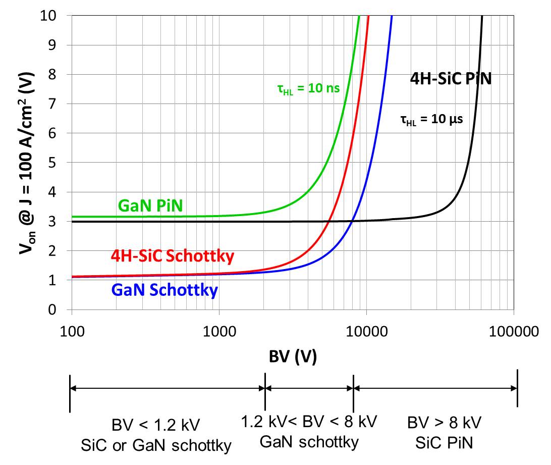
Fig. 1. Forward voltage drop as a function of BV.
The calculated on-state voltage drop (VF) as a function of breakdown voltage is shown in Fig. 1. At low BV (< 2 kV), SiC and GaN SBDs have the lowest voltage drop (~ 1.2 V), limited by the turn-on voltage of the Schottky junction. When BV increases, (between 2 and 8 kV), the voltage drop across the drift region becomes dominant because of absence of conductivity modulation in a unipolar SBD. In this voltage range, GaN SBDs have a lower VF than SiC SBDs because of a higher critical field in GaN. For BV > 8 kV, the SiC pin has the lowest voltage drop due to conductivity modulation which minimizes the voltage drop across the drift layer. Recombination lifetime in GaN is very low due to its direct bandgap which causes a fast radiative recombination. The high turn-on voltage and absence of conductivity modulation leads to a prohibitively high VF for GaN PiN rectifiers.
Commercial SiC diodes are typically Junction Barrier Schottky (JBS) diodes where p islands are inserted in the Schottky junction area. JBS diodes retain the low VF and negligible QRR characteristics of SBDs, but have lower off-state leakage current and improved surge current capability (IFSM). In a JBS diode, the Schottky junction turns on at low voltage and conducts current under normal operating conditions. However during a surge current pulse, the pn junction can turn on and minority carriers are injected into the drift layer. The subsequent increase in the conductivity of the drift layer minimizes the increase in VF resulting in a low surge energy loss and a high IFSM capability of SiC JBS diodes. By contrast, GaN Schottky or JBS rectifiers cannot enter a bipolar conduction mode due to the low carrier lifetime. This is a key disadvantage of a GaN power rectifier even though its on-state power loss is lower than SiC due to the superior critical field of GaN.

Fig. 2. Maximum current density for different rectifier technologies
