


LIBRARY
Ultra-Low Inductance Vertical Phase Leg Design with EMI Noise Propagation Control for Enhancement Mode GaN Transistors
Year: 2016
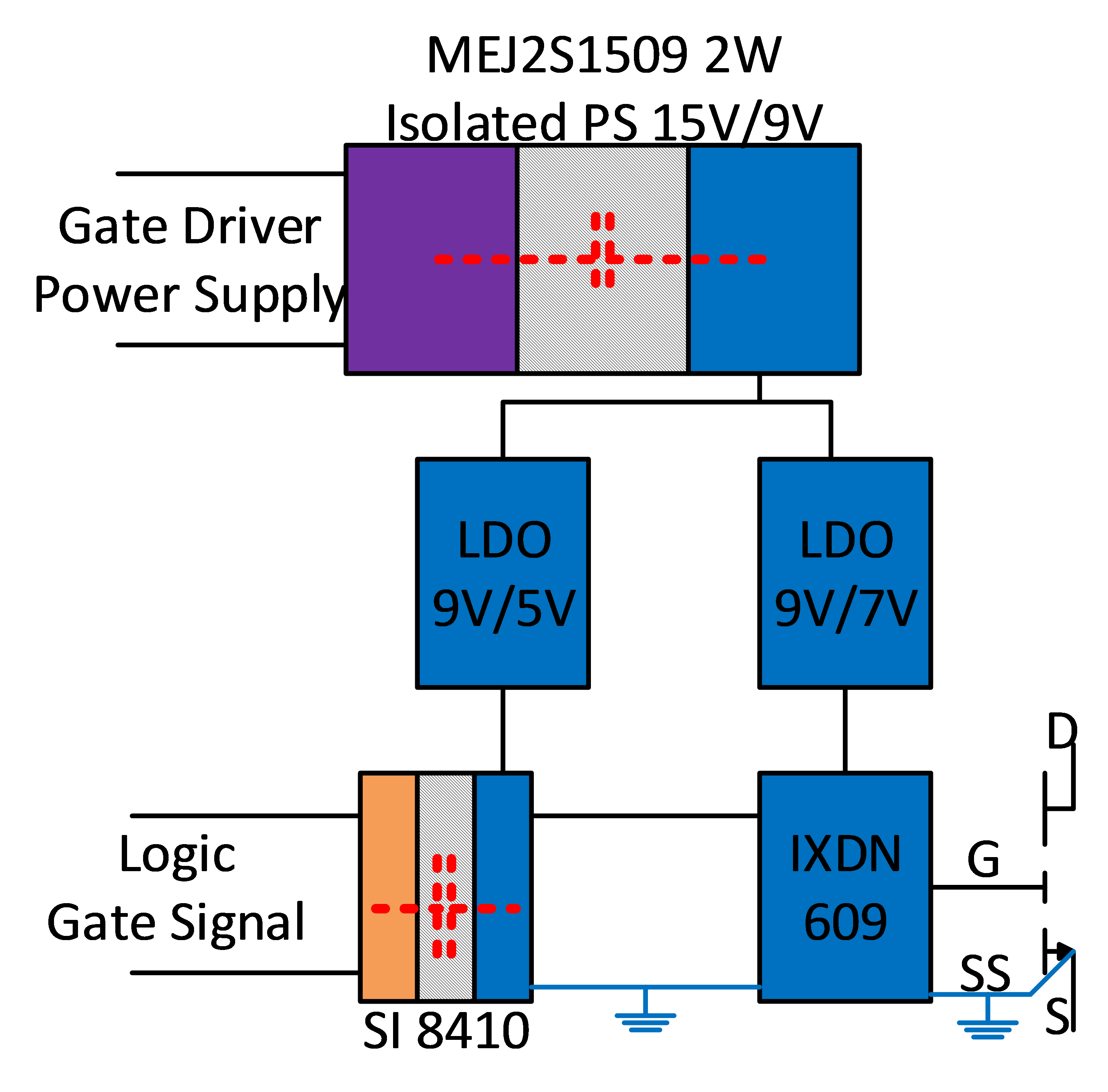
Fig. 1. (a) Gate driver circuit design
The high switching speed of GaN devices will generate a high dv/dt that can induce high CM current that propagates from power loop to gate loop. The main propagation path is through the stray capacitance of the isolated power supplies and digital isolators as shown in Figure 3. In order to improve the electromagnetic compatibility of the system, CM noise propagation is controlled by differentiating the propagation path impedance of the digital control circuits and their power supply circuits. The block diagram is shown in Figure 1, where digital isolators with ultra-low isolation capacitance are selected for both top and bottom devices to provide good isolation for high frequency EMI noise. The power supply of the digital control circuit is also selected with an ultra-low isolation capacitance to create a high impedance path to reduce CM noise current through the digital control circuits. Meanwhile the gate driver power supply is selected with a relatively higher isolation capacitance to create a lower impedance path for CM noise. In addition, CM chokes are added to both the signal and power supply path to maintain a higher impedance at high frequency. The selection of the choke impedance also needs to ensure that the digital control circuits have a higher noise propagation path impedance than its power supply. In this configuration, the digital control circuit will have an ultra-high propagation path impedance and the gate drive power supply will provide a bypassing path with a relatively low propagation path impedance in parallel with the digital control circuits which can effectively reduce CM noise current through the digital control circuits. With the proposed design, gate drive power supply circuits will sustain the high CM current, however, the power supply control circuits should have higher susceptibility and noise immunity considering its relatively smaller dimension and higher circuit integration level.
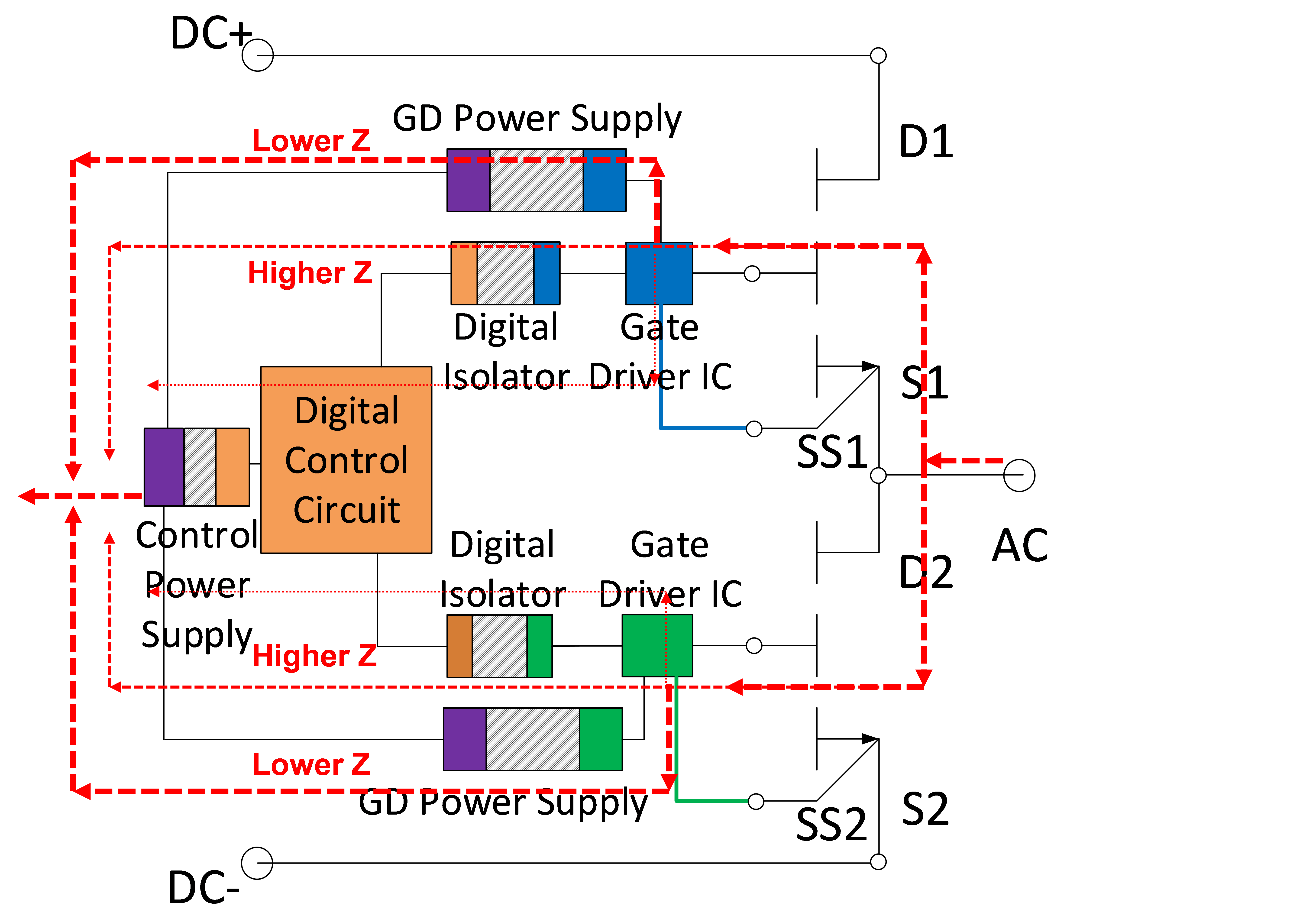
Fig. 1. (b) Gate driver circuit design with CM noise propagation control
