LIBRARY
Driving and sensing design of an enhancement-mode-GaN phase-leg as a building block

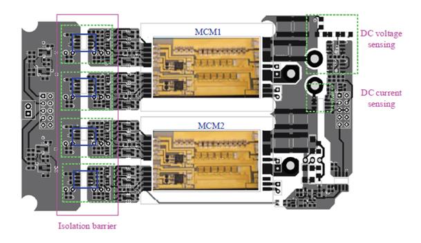
The key to designing the driving channel with high common-mode transient immunity (CMTI) is to provide a high impedance between the high-voltage/high-power side of the GaN MCM to the low-power side that comes from the control circuit. The power supply and the gate drive are selected with very small inter-capacitance, whose effect is illustrated in Fig. 2. A Y-capacitor filter is added to avoid noise flowing into DSP control board. Additionally, the PCB layout is considered. For example, to minimize the parasitic capacitance generated by the layout, the copper layers of the primary side and secondary side should be without overlap.
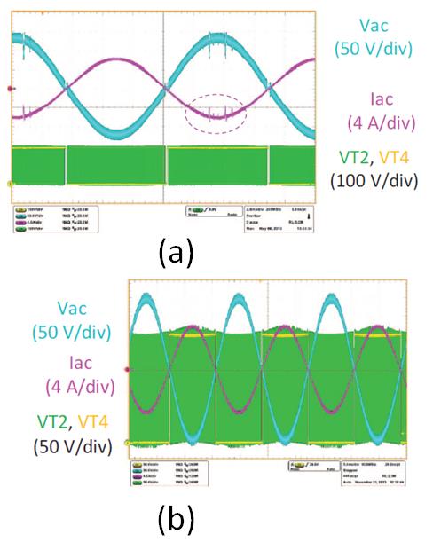
In order to achieve reliable sensing in the very noisy GaN switching environment, the DC voltage sensor requires a low-pass filter stage and needs to be placed outside the full-bridge board; the AC current sensor should not be separated from the switching node by a high-impedance component, such as an inductor, and therefore will also be outside the full-bridge board, while the DC current sensor can be left on the full-bridge board. Inverter tests are performed with 300V, 6A and 500kHz, with and without the techniques implemented; the sensing results are shown in Fig. 3. These clean sensing results are critical to the closed-loop control of the system.


