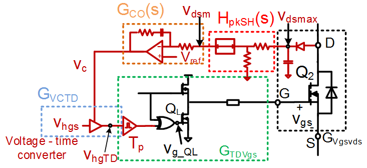
Fig.1. Proposed ORAS and its functional blocks. Peak detector senses vds into vdsmax. vdsm is the sampled output of voltage divider and sample-and-hold from vdsmax. Vref and vdsm are compared in a PI-controller. Controller output vc decides the time delay from vhgs to vhgTD. A delay self-clamping signal vg_QL drives QL and changes vgsmin. vgsmin alters vdsmax.
Voltage overshoot is regulated by controlling the gate driver. During the device turn-off, voltage ringing occurs on the switching devices due to the resonance between parasitic elements. Improvements can be achieved by slowing down the gate driving speed or by energy absorption by passive components, but switching loss will increase when using these methods. Controls of gate drivers can reduce voltage with less power loss, but the clamping voltage varies with different parameters or operating conditions in the applied circuit. This paper presents a gate driver with overshoot regulation and active snubbing (ORAS). Minimum energy is used to achieve voltage clamping within the expected level. It regulates overshoot with controlled gate-signal at the beginning of ringing, so voltage can be clamped by the least energy loss. To limit the maximum voltage, a closed-loop controller is used to clamp the voltage to be under a certain level by sensing the peak voltage. Through simulation, ORAS is proven to reduce voltage overshoot from 28 V to 17 V, and regulate V
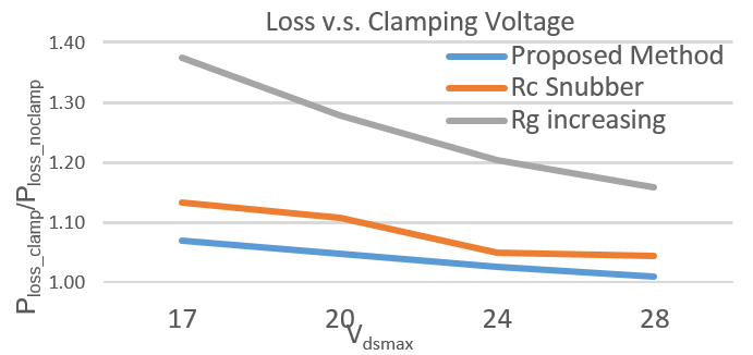
dsmax within 1 V of error during the load/line transient. Compared with other methods in the same level of voltage-clamping, ORAS consumes only half of the energy by using a snubber and 1/6 of the typical energy used by increasing gate resistance. With precise overvoltage regulation and minimum energy consumption, we built a gate driver with an overshoot regulator.
We developed an overshoot regulator on the gate driver to control vds stress on the device during low-side turn-off. Compared with existing methods, the ORAS only needs negligible energy to clamp overshoot. Peak voltage vdsmax can be regulated with a closed-loop feedback by controlling the timing of Self-Clamping.
The proposed regulator is simulated on a synchronous buck converter, which is proven to be stable for different values of V
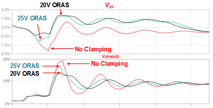
dsmax, loads and line transients. By increasing the snubber, maximum vds is reduced from the original 29 V to 20 V by ORAS and 1/6 of the loss is achieved by increasing gate resistance. Furthermore, the EMI level is 12dB lower in the FM frequency band by using ORAS.

Fig. 2. Top: Vds and Vgs waveforms under 20 V, 25 V regulation, and no overshoot regulation. Bottom: Vdsmax = 19.8 V, 25.1 V, 28.8 V in 20 V, 25 V, and no regulation.

Fig. 3. Fig. 3. Power losses in different voltage reduction methods. When Vdsmax is 20 V, the loss in the ORAS is reduced to 1/2 the loss by using the RC snubber, and 1/6 loss by increasing Rg.
