LIBRARY
Evaluation and Applications of 600V/650V Enhancement-Mode GaN Devices

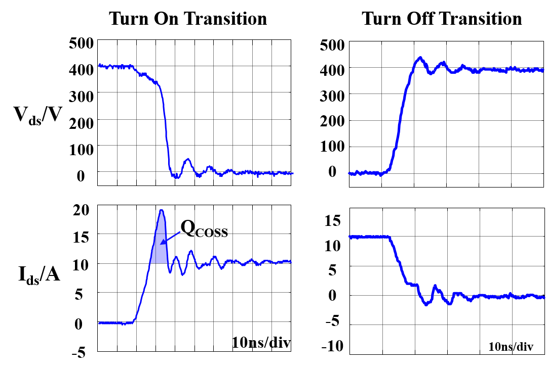
Understand the switching characteristics of GaN switches is essential in order to use GaN devices correctly and efficiently in circuit design. Figure 1 shows the typical switching waveforms of the control switch in a half-bridge configuration based circuit. During the turn-on transition, a large current overshoot is induced by the junction capacitor charge of the free-wheeling switch. The integration of voltage and current during the turn-on transition generates significant power dissipation, which is in the magnitude of tens of uJ. On the other hand, the cross time of the drain-source voltage and current during the turn-off transition is quite short. The channel of the GaN can be easily pitched off since the GaN device has a relatively high transconductance. The majority of the drain-source current measured from the terminals is actually used to charge the junction capacitors voltage to the steady-state value and this part of stored energy is either dissipated during the hard-switching turn-on transition or recycled to the source during the soft-switching turn-on transition. Both packaging related to parasitic inductance and gate resistance of the gate driving circuit have a significant impact on the switching loss of e-mode GaN devices. In general, the turn-on switching loss is much higher than the turn-off switching loss for e-mode GaN devices and ZVS turn-on is desired to fully exploit the advantages of the e-mode GaN de-vices.
The switching speed of e-mode GaN devices in terms of dv/dt and di/dt, is 3-5 times higher than that of the Si MOSFETs. The gate drive circuit should be carefully designed to avoid the issues brought by high di/dt and dv/dt. The di/dt issue is cause by a high current slew rate on the parasitic inductance which fights against the gate driving circuit. The best way to solve the di/dt related issue is to minimize the device package and PCB layout parasitic inductance. The dv/dt issue is caused by the common mode current coming through the high side driving circuit and deteriorating the input PWM signal. Resolution requires minimal parasitic capacitance between the high side and the signal ground, as well as minimized input impedance.
One advantage of e-mode GaN over cascode GaN at soft-switching condition is the smaller junction capacitor charge which requires less circulating energy. The related power loss is considerable at high frequency. The superb performance of e-mode GaN device make it suitable for a wide range of applications. This paper takes a low power adapter and a 1kW LLC converter as examples to show the impact of GaN devices on system design. The potential impact of GaN goes beyond the simple measures of efficiency and power density. It is feasible to design a system with a more integrated approach at higher frequency, and therefore, it is easier for automated manufacturing. This will bring significant cost reductions in power electronics equipment and unearth numerous new applications which have been previously precluded due to high cost.


