


LIBRARY
Dynamic Characterization of 650 V GaN HEMT with Low Inductance Vertical Phase Leg Design for High-Frequency High-Power Applications
Year: 2016
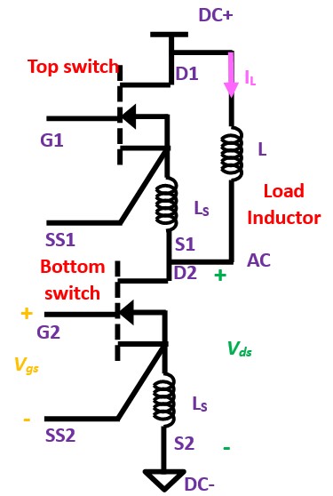
Fig. 1. Phase leg schematic for DPT with inductor across top switch.
The phase-leg schematic is shown in Fig. 1 with an inductor across the top switch. In the vertical phase-leg design, the top/high-side switch is mounted on the top layer of the PCB, whereas the bottom/low-side switch is mounted on the bottom layer of the PCB, as shown in Fig. 3. The power loop inductance is thus limited only by the device package inductance, the dimensions of the device and the PCB. Compared to the reference lateral power loop layout (the two devices of the phase leg are mounted side-by-side on the same layer of the PCB, as shown in Fig. 2), this design has lower power loop inductance and minimized coupling between the gate loop and power loop, as the gate loop is perpendicular to the power loop. In contrast, in the reference design the gate loop is parallel to the power loop, and the AC and DC terminals are coupled with each other. The proposed design has minimal coupling between the AC and DC terminals of the phase leg.
A double-pulse test of the proposed design was conducted with the load inductor connected across the top switch. The external gate resistance is 10 ω, as recommended. The bottom switch was turned on and off (with 5 µs dead time), while the top switch was kept off. The gate driver is designed for on-state Vgs 7 V and off-state Vgs 0 V. The results at 400V DC voltage, 30 A inductor current were measured. The Vds overshoot measured was 68.8V (17.2%), whereas from the double-pulse test results in the lateral power loop design under similar conditions, the Vds over-shoot is 188 V (47%). Thus the vertical design can reduce the voltage overshoot to less than half that of the lateral power loop design. This low overshoot paves the way for reduction of gate resistance, faster switching and hence lower energy losses.
Fig. 2. Reference lateral phase-leg design.
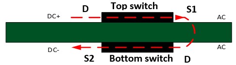
Fig. 3. Vertical power loop design.
