Become a Member
Become a Member

LIBRARY

A New Package of High-Voltage Cascode Gallium Nitride Device for High-Frequency Applications

Year: 2016
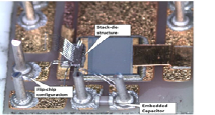
Fig. 1. A prototype of the proposed package for high-voltage cascode GaN device with new features.
The emerging gallium nitride (GaN)-based wide bandgap (WBG) semiconductor devices have been developed for power conversion applications, such as point-of-load converters, electrical vehicle chargers, and solar inverters. The dominant type of commercial high-voltage ( 600 V rated) GaN power devices is the high-electron-mobility transistor (HEMT) fabricated in a lateral aluminum gallium nitride/gallium nitride (AlGaN/GaN) heterojunction structure. In this configuration, the GaN HEMT possesses a high breakdown field and high saturation electron velocity, while polarization charges at the AlGaN/GaN heterointerface generate a high-concentration two-dimensional electron gas (2DEG) with high carrier mobility, and thus significantly reduce the on-state resistance. Therefore, high-power-density GaN HEMT devices, which are more efficient than the incumbent silicon (Si) based devices, can be switched faster with lower switching losses. GaN-on-Si transistors are expected to offer the best cost-performance ratio among all WBG-based semiconductors developed in various structures [6], [7]. However, the packaging of GaN HEMT devices has become one of the significant limiting factors to reaching the full potential of this WBG semiconductor. A high-performance package with minimized impacts on the electrical and thermal properties of the GaN bare-die device has to be invented in order to compete with Si technology.

In this study, the switching characteristics and thermal performance of a commercial cascode GaN device in a traditional PQFN package are firstly considered for megahertz (MHz) operation. Then, a new package of this normally-off GaN device configured in the same cascode structure is created. A 600 V lateral GaN HEMT is co-packaged with a 30 V vertical Si MOSFET in the stack-die structure with the optimized arrangement of bonding wires. A balancing capacitor is also integrated into the device package in order to compensate the junction capacitance mis-match between the GaN and Si devices. The flip-chip configuration is realized in this advanced package for easy and effective thermal management as well as better reliability. The whole pack-aging of the high-voltage cascode GaN device is still contained in a PQFN format with the new features listed above. Finally, this cascode GaN device in the newly developed package has demonstrated better switching and thermal performance than the equivalent commercial product packaged using the same GaN HEMT and Si MOSFET chips.

Fig. 2. Temperature distribution of stack-die packaged cascode GaN device in flip-chip configuration: (a) Top view; and (b) Cross-sectional view.

Our Industry Partners