LIBRARY
2 W Gate Drive Power Supply Design with PCB-Embedded Transformer Substrate

To pursue a small inter-capacitance (isolation capacitance) from the primary to the secondary side in the transformer, the primary and secondary windings should be located as far apart as possible. Accordingly, as the transformer volume increases, it exacerbates the difficulty in achieving high power density. The challenge of this work is to find an appropriate design approach, aimed at small converter volume, small inter-capacitance and high efficiency.
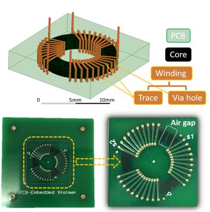
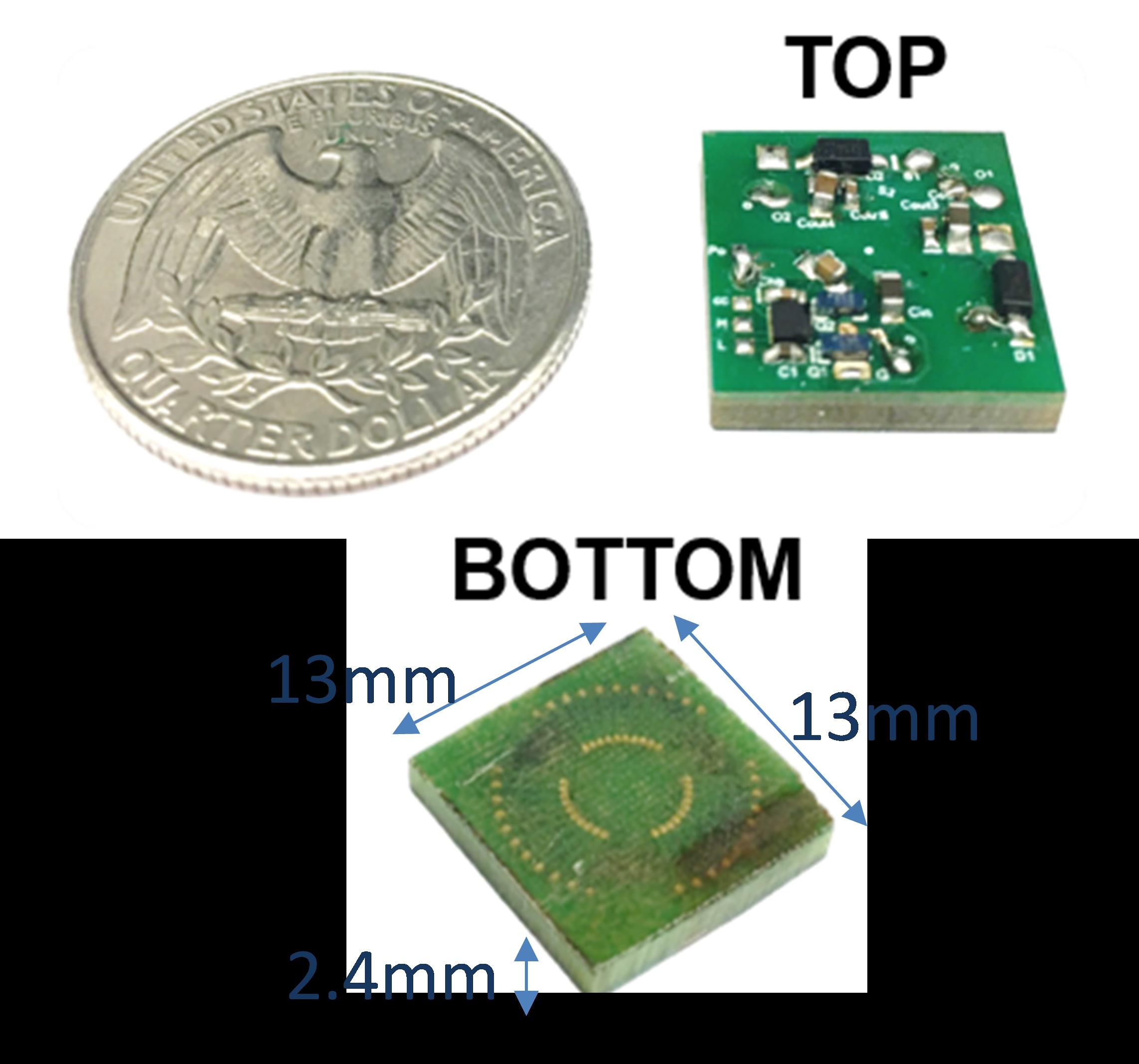
To design the targeted gate driver power supply, the paper first presents the circuit design, including the topology selection, operation mode analysis, and active and passive component selections, operation mode analysis, and active and passive component selections. The PCB-embedded transformer structure is then illustrated in Fig. 1, and the core and PCB material selections are addressed. To find a compromise among a low inter-capacitance, low transformer loss, and a small volume, an optimization of the transformer dimensions is performed based on the transformer models. With the optimized dimensions, the transformer is built and shown in Fig. 2, and the fabrication procedures, including the standard lamination process, are introduced. The transformer and the converter hardware are showin in the end and characterized with experimental waveforms, efficiency, isolation voltage, inter-capacitance, and total volume.


