LIBRARY
Design and Development of a 10 kV, 60 A SiC MOSFET Module

At present the performance of these unique devices is limited by standard module packages that were originally developed for slower, lower density Si devices. The aim of this work is to develop a high-density, high-speed, half-bridge module for these 10 kV SiC MOSFETs without antiparallel diodes; instead, the reverse current will flow through the MOSFET channel, and the body diode will only conduct during the deadtime. There are several challenges associated with this objective. In particular, the desire for high density will increase the electric field concentration within the module. This is a new challenge that has not been explicitly addressed before, and it arises from the development of this high-density, high-voltage SiC device.
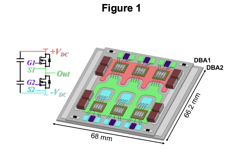
The designed power module is shown in Fig. 1. The module consists of AlN direct bonded aluminum (DBA) substrates, and uses 96.5Sn/3.5Ag solder preform for the die attach, and 10-mil Al wirebonds for the interconnections. Embedded decoupling capacitors are also included in the module for improved transient performance. According to ANSYS Q3D Extractor, the gate- and power-loop inductances are 6 nH and 10 nH, respectively.
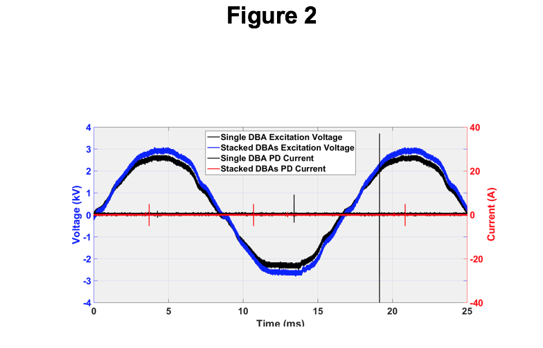
To minimize the peak electric field that occurs at the triple point of the DBA substrates, two DBAs are stacked together. Partial discharge (PD) tests were performed for both the single- and stacked-substrate cases. When stacking two DBAs together, the partial discharge inception voltage (PDIV) increased by 15 %. This can be attributed to the reduction in the electric field at the triple point. Fig. 2 shows the PD signals for both cases.
Another challenge associated with the high-density design is the module termination. Specifical-ly, how to interface the module with the rest of the high-voltage system. Commercial high-voltage connectors are significantly larger than the module itself, and are thus not viable options for this work. Consequently, alternative solutions need to be explored, and evaluated based on the tradeoffs between peak electric field, current carrying capability, parasitic inductance, ease of assembly, and reliability.


