


LIBRARY
Phase Leg Design and Dynamic Characterization with two 650 V/ 60 A GaN HEMTs in parallel
Year: 2017 | Author: Nidhi Haryani | Paper: D3.12
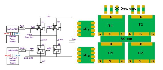
Fig. 1. (a) Phase leg schematic and (b) Phase leg block diagram
However, the rated current for commercially available GaN devices is limited to 60 A. The on-resistance also increases a lot with current and temperature thus resulting in very low efficiency for high current applications. Hence, paralleling multiple GaN devices is required for high efficiency high power applications.
The schematic and layout design for two GaN devices in parallel for both phase leg and DPTer are shown in Fig 1. The 650 V/ 60 A GaN device discussed in this paper has a very small package inductance but to fully extract the benefits of this small package, it is important to design the gate-source loop and power loop layouts to have minimum parasitic inductances. Also when paralleling multiple GaN devices, it is important to design identical gate loop and power loop for both the devices. Furthermore, the layout should be designed so that there's minimal parasitic inductance in between the two devices.
The recommended design from GaN Systems is shown in Fig.1 , which is based on the schematic. However, the layout design guidelines presented in this paper are not discussed in any previous work in detail. A detailed dynamic characterization of the above mentioned design and the problem of circulating current during turn-on transient is observed. The issue of circulating current has not been discussed in any previous work. The limit of this DPTer design is tested and findings show that due to the parasitics added by the current shunts, the design's current limit is much lower than the case when the shunts are shorted. The methods to control the circulating current are also discussed.
