


LIBRARY
Wide-Input-Voltage-Range Dual-Output GaN-based Isolated DC-DC Converter for Aero-space Applications
Year: 2017 | Author: Xingye Liu | Paper: D3.4
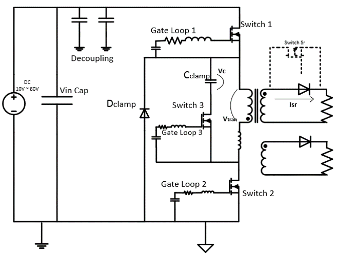
Fig. 1. Converter topology
With the current topology and operation level, the main challenge is efficiency over a wide range of input voltage. Even though the lowest and highest input occur at start-up and transient re-sponse, maintaining efficiency for input voltages from 18V to 70V still requires a significant tradeoff in design. In addition, the potential ability for control should be checked in order to limit the duty cycle to a reasonable range. In terms of efficiency, switches (or diodes) and transform-ers are the two main components responsible for most of the power loss. By selecting proper devices and designing a customized transformer, the whole range loss is controlled, but there is still some sacrifice at specific operation points.
In terms of manufacturing, the layout is critical, and gate driving loops for such devices on the primary side are more sensitive to noise than other converters. The final version of the converter has optimized the gate driving loop inductance and the layout is optimized for a smaller size and better power loop design.
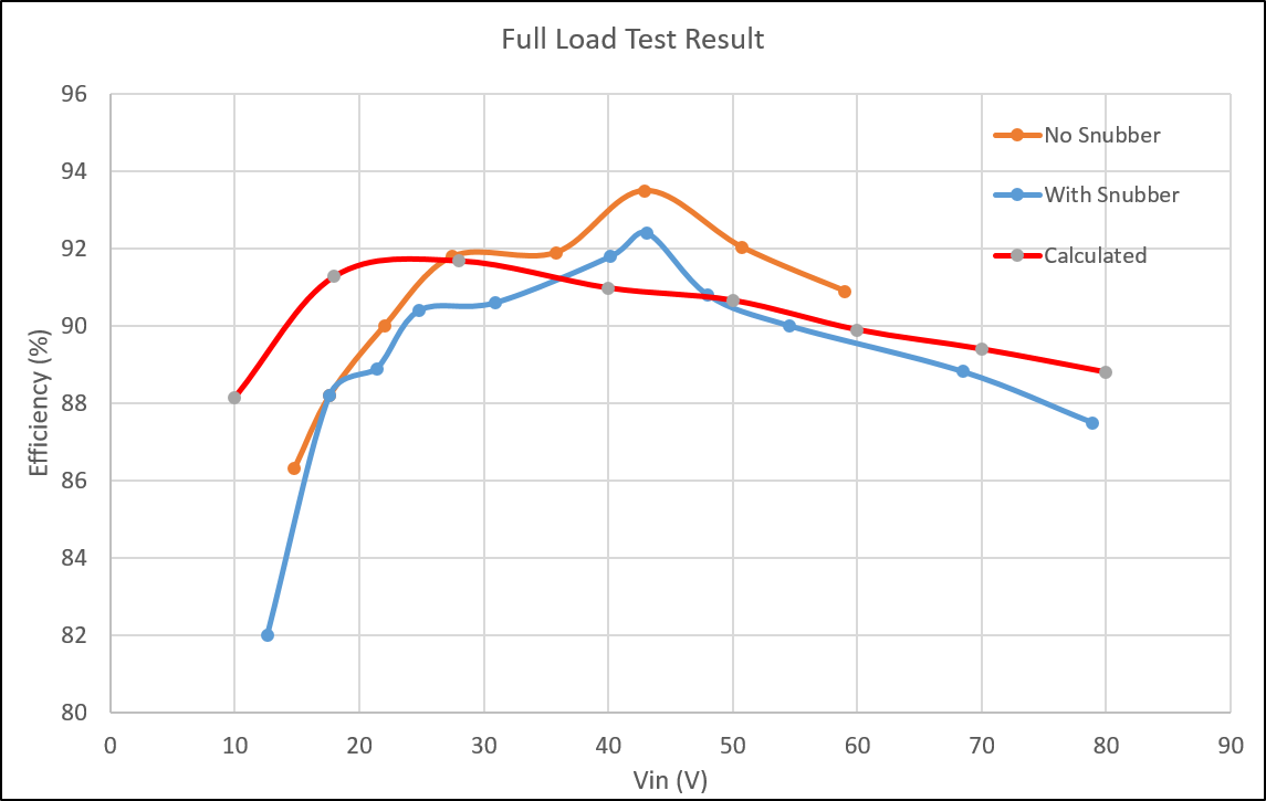
Fig. 2. Converter efficiency
