


LIBRARY
Design of a SiC-Based Modular Multilevel Converter for Medium Voltage DC Distribution System
Year: 2017 | Author: Jianghui Yu | Paper: D4.1
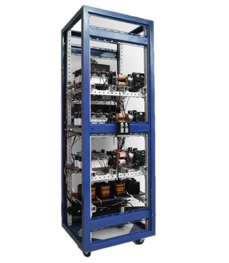
Fig. 1. Hardware prototype of a MMC
Currently, Si IGBTs are largely used in this type of converter, in accordance with its low switching frequency requirements and relatively low power density. The latter is perhaps its main shortcoming. This, however has been recently overcome by developing new high frequency and switching-cycle PWM and control schemes that allow the MMC circuit to profit from a high switching frequency operation and achieve high power density. Wide- bandgap (WBG) devices, such as SiC, have consequently become a viable option enabling engineers to fully exploit the benefits of this power conversion solution for MVDC systems.
The converter prototype is shown in Fig. 1. It is able to operate as an inverter or a rectifier with minor control system modifications. Unlike the traditional MMC, there is only one PEBB per arm in the converter shown in Fig. 1 thanks to the use of fast SiC devices. This configuration retains the main properties featured by the MMC, such as distributed energy storage. Despite the reduced number of PEBBs, the converter's passive components do not suffer from harsher requirements due to the fast switching speed of the SiC devices employed, specifically 1.7 kV SiC MOSFETs. In effect, by increasing the switching frequency, the converter still has a high equivalent switching frequency without requiring multiple series-connected modules. With it, a 1 kV DC bus can be generated, which is under consideration for use in commercial and military marine applications. Higher voltages can easily be achieved by increasing the number of PEBBs per arm.
The PEBB design, control methods and hardware, pre-charge and discharge, protection will be included in the final paper.
Different functional tests need to be conducted throughout the design and construction process. First, each busbar undergoes a High Potential (HIPOT) test to verify the insulation. They can withstand at least 6 kV from positive to neutral or negative to neutral. Then the Double Pulse Test is performed on every top or bottom switch of the SiC module and every channel of the gate driver to verify the switching performance and protection action. It is tested under a 1 kV drain-source voltage and a 50 A drain current, which is close to normal operation. Then each PEBB is operated as an inverter with an open-loop control to verify the modulation and thermal behavior. Fig. 2 shows the primary test results of the whole converter prototype, including capacitor voltages, arm currents and circulating current from the same phase and three-phase ac current. It was operated as an inverter with a 300 V DC source.
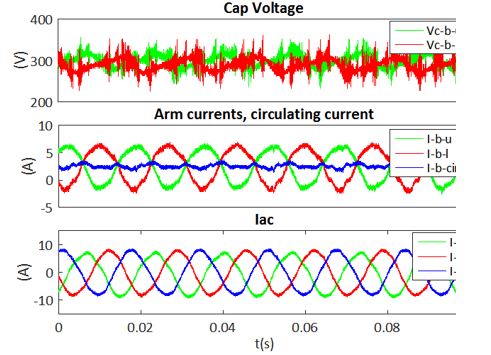
Fig. 2. Inverter test results
