LIBRARY
DBC Switch Module for Management of Temperature and Noise in 220-W/in3 Power
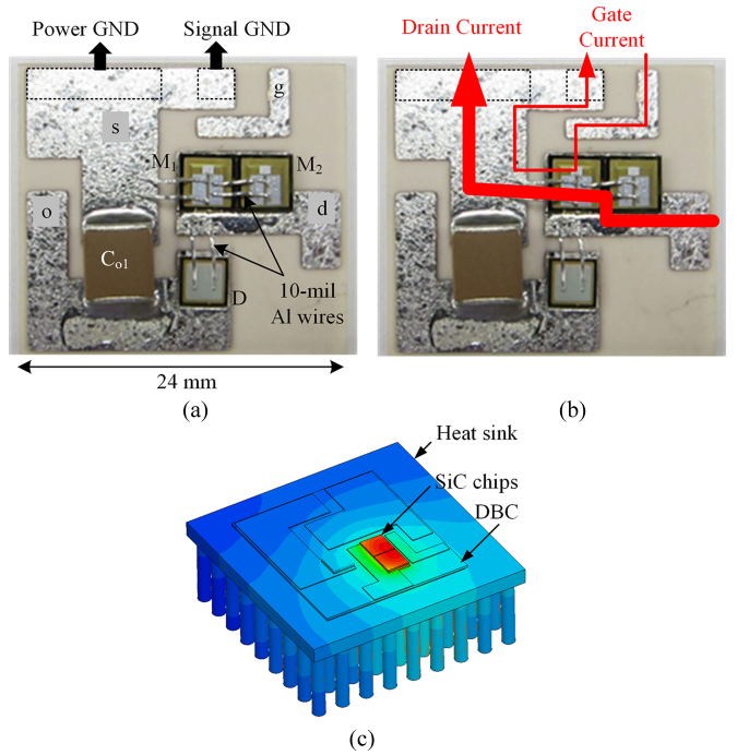
Comparing a PCB module with a GaN MOSFET, the SiC DBC module in Fig. 1 shows a higher thermal conductivity. The thermal behavior of the DBC module was simulated by Ansys ePhysics to inspect the maximum junction temperature of semiconductor chips and junction-to-case thermal conductivity. Fig. 1 (c) shows that the junction temperature is 65.1°C and the heat sink temperature is 55.7C when each MOSFET die has a 3.75-W power loss. Junction-to-case and case to-heat sink thermal resistances are calculated as 0.89 and 1.46°C/W, respectively. The total thermal resistance from junction to heat sink is 2.35°C/W, 63% of the 3.71°C/W for PCB module.
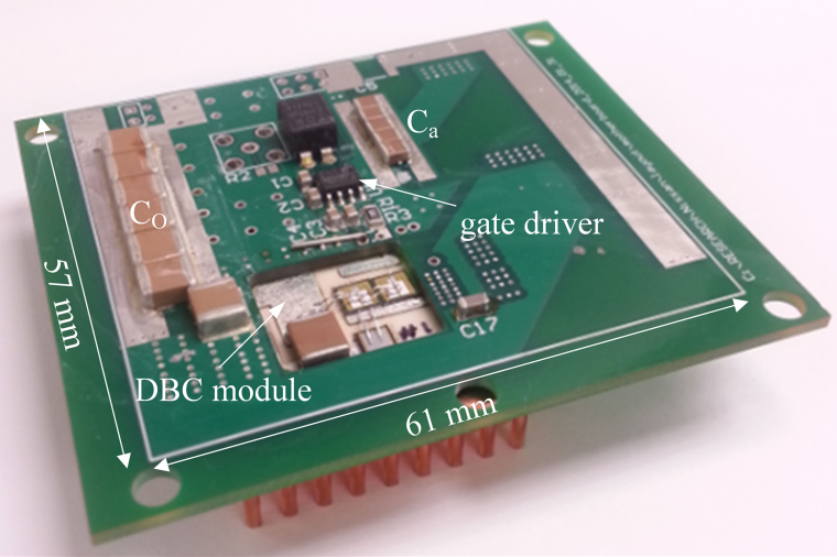
The ZVS boost converter using a DBC module is shown in Fig. 2. Capacitors and a gate driver were placed on the top side of the motherboard. Area of 57 mm 61 mm or 3477 mm2 was utilized. A fan, power supply for gate driver, and the magnetic components were assembled to the bottom side of the motherboard fixing the height of the converter as 43 mm. The volumetric power density PD with 2-kW output power is calculated as PD = 2000 W/(3477mm2 43mm) = 220 W/in3.
