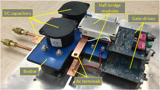
Fig. 1. Final assembled PEBB with double-sided bus-bar
The concept of a power electronics building block (PEBB) is the integration of fundamental components, such as power devices, gate drives, and control schemes. This allow for numerous power conversion topologies to be implemented by a series/parallel connection of these building blocks to achieve practically any desired current/voltage/power level, and is therefore able to be used in a variety of applications. Although SiC-based PEBBs are capable of operating at high switching frequencies and high power levels, the high-speed switching transients within the PEBB are strongly affected by the resistance and inductance of the connections between components. The large stray inductance in the PEBB may cause excessive transient voltage overshoots across the MOSFETs. The voltage overshoots can result in increasing power loss, high voltage stress, and exceed the MOSFET safe operating range. Stray inductance is hence an important concern in the design of high-power and high-frequency power converters. The busbar technology is an effective way to reduce interconnection inductance. It consists of stacking several copper sheets, each separated from the other by a dielectric material. The role of the dc link busbar of the PEBB is to achieve a series or parallel configuration of the capacitors and to link the dc capacitor bank and power modules. In addition to its low impedance (both inductance and resistance), using a busbar improves the thermal performance, since the surfaces of exchange are increased, and heat transfer is facilitated. Furthermore, adding thick external layers to the busbar improves the mechanical strength of the busbar without affecting its impedance. Lastly, busbar connections contribute to a compact size, which is a critical aspect of the PEBB design.
This paper presents a study of busbar optimization for a high-power and high-switiching-frequency SiC-based H-bridge PEBB. A new double-sided busbar with symmetric minimized commutation loops is presented, which eliminates the use of the decoupling capacitors and also results in improved thermal and switching performance of the PEBB. Step-by-step busbar design guidelines are provided with all the necessary equations and analysis to select the materials and calculate the dimensions of the different layers. Furthermore, the stray inductance of the current commutation loops is estimated by simulation and verified experimentally. The power stage model of the PEBB is also developed including busbar parasitics. Finally, the switching performance of the PEBB is presented to show the effects of the minimized loop inductance on the switching transients.

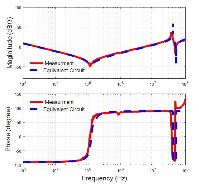
Fig. 2. Power stage impedance result from measure-ment and equivalent circuit of the PEBB
