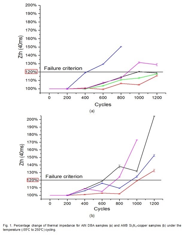
Fig. 1. Percentage change of thermal impedance for AlN DBA samples (a) and AMB Si3N4-copper samples (b) under the temperature (-55o C to 250o C) cycling.
Demands for higher power density and reliability in power electronics systems are driving the need for the development of high-temperature packaging solutions. Existing power module packaging technologies that rely on lead-tin or lead-free die-attach solders, and alumina direct bond copper (DBC) insulated substrates are limited to 125 ° C junction temperatures for reliable module operations. Recently, die-attach by silver sintering, or the low?temperature joining technique, has been shown to significantly improve chip-bonding reliability at higher junction temperatures. Concurrently, direct-bonded aluminum (DBA) substrates with aluminum-nitride (AlN) ceramic and active metal brazing (AMB) substrates using high-toughness silicon-nitride ceramic are shown to be significantly more reliable than alumina DBC substrates, especially over large temperature swings. However, it is reported that the surface roughness on both substrates grew with the number of temperature cycles. The roughening rate on the DBA substrate was two times faster than that on the AMB substrate. This may cause reliability issues. To evaluate the effect of surface roughening on the sintered-silver joint reliability, we measured the transient thermal impedance of the bonded power chips. As shown in Fig. 1, despite the higher roughening rate, the sintered-silver bond on the DBA substrate had a longer lifetime than that on the AMB substrate.
Fig. 2 is the cross-sectional scanning electron microscopy, which shows the formation of vertical cracks in the sintered bond-line on the DBA substrate, as opposed to horizontal cracks on the AMB substrate. Formation of the vertical cracks in the bond-line relieved stresses without significantly impacting the thermal performance.
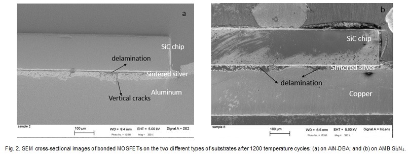
Fig. 2. SEM cross-sectional images of bonded MOSFETs on the two different types of substrates after 1200 temperature cycles: (a) on AlN-DBA; and (b) on AMB Si3N4.


