LIBRARY
Advanced Power Module Packaging (1998)
Year: 1998
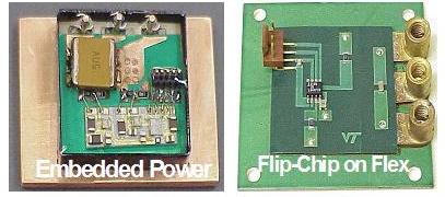
CPES is promoting the idea of replacing the conventional wirebond with direct bonding, and has introduced a number of techniques, such as the flip-chip-on-flex and the embedded power technology. These integration approaches feature much-reduced interconnect parasitics, which enhance circuit performance; improved thermal management by introducing the opportunity for double-sided cooling; and improved functional integration by integrating snubber capacitors, bus capacitors, chip inductors, and incorporating embedded current sensors into the multi-chip, multi-layer packaged module.
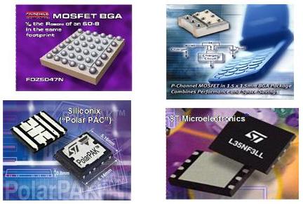
In late 2002, industry began to introduce a range of products that utilized packaging techniques similar to what CPES developed earlier, including Fairchild's bottomless and BGA packaging, Renesas's lead-free packaging (LFPAK), International Rectifier's FlipFet and DirectFET, Siliconix's PowerPAK, and STMicroelectronics's FLAT package. Features typically claimed in these new products include reduced contact resistance, reduced parasitic inductance, and improved thermal management, which are what CPES reported in the literature a few years ago. These packaging technologies (wire-bondless) have become the mainstay of the new generation of power devices/packaging.