LIBRARY
Fabrication and Characterization of a High-Density, Planar 10 kV SiC MOSFET Power Module

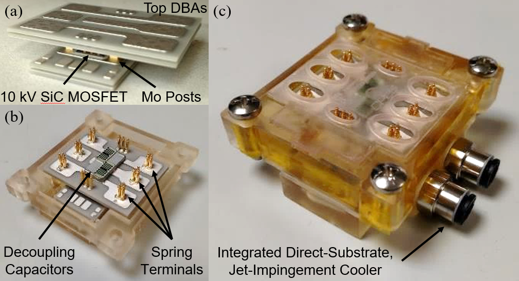
Fig. 1 shows the fabricated half-bridge module, which has two 10 kV, 350 m&Omega die. The module has a planar structure, using molybdenum posts (Fig. 1 (a)) and a direct-bonded aluminum (DBA) substrate (Fig. 1 (a)) as the die interconnection instead of wirebonds. In order to address the enhanced electric fields associated with a high-voltage, high-density package, two DBAs are stacked on top of each other. By stacking the two DBAs, the electric fields both within the ceramic and at the critical triple pointswhich, in this case, are where the ceramic, metal, and encapsulation meetare drastically reduced. To further reduce the power loop inductance, wo series decoupling capacitors are placed directly above the MOSFETs (Fig. 1(b)). The module also features a custom-designed, direct substrate, jet impingement cooler that is integrated into the housing (Fig. 1 (c)).
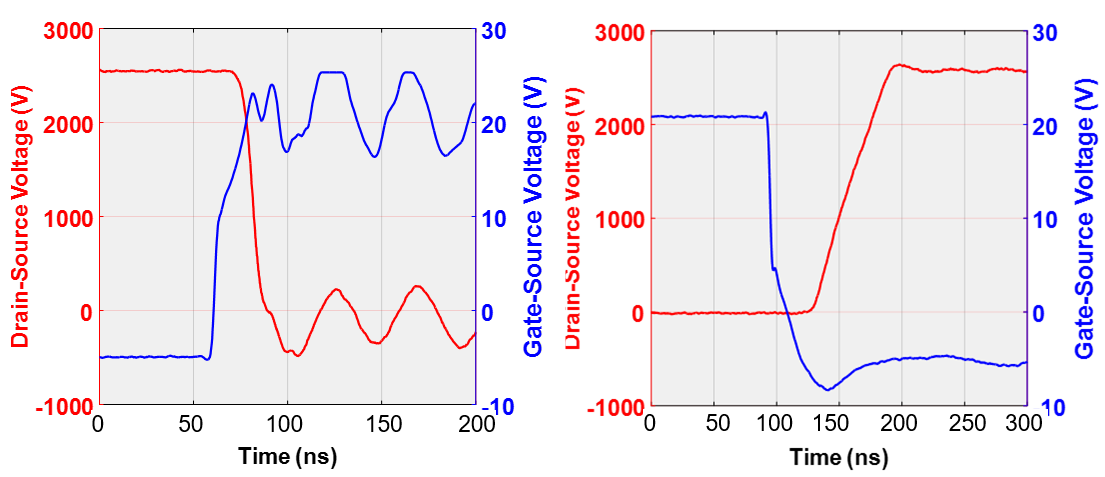
Double pulse tests were performed on the fabricated module to evaluate its switching performance. The tests were conducted up to 2.5 kV and 12.5 A with no external gate resistance (Fig. 2). The voltage was limited to 2.5 kV due to the voltage rating of the test rig bulk capacitors (2.7 kV). The voltage fall time during the turn-on transient is 10 ns. This gives a dV/dt of 200 V/ns. The voltage rise time during the turn-off transient is 47 ns, which gives a dV/dt of 43 V/ns. The voltage overshoot is less than 2 percent at turn-off, indicating a low-power loop inductance.
To evaluate the performance of the integrated direct substrate, jet impingement cooler, thermal impedance measurements were carried out. The lowest junction-to-ambient specific thermal resistance of the module was measured to be 26 mm2K/W (0.38 K/W) for a flow rate of 0.47 l/min. Preliminary partial discharge tests were also performed to evaluate the electrostatic performance. The tests showed that by stacking two DBAs and connecting the middle metal layer to half of the dc bus voltage, the partial discharge inception voltage could be increased by 87 percent.


