


LIBRARY
Design and Development of a High-Density, High-Speed 10 kV SiC MOSFET Module
Year: 2018 | Author: Christina DiMarino | Paper: D1.6
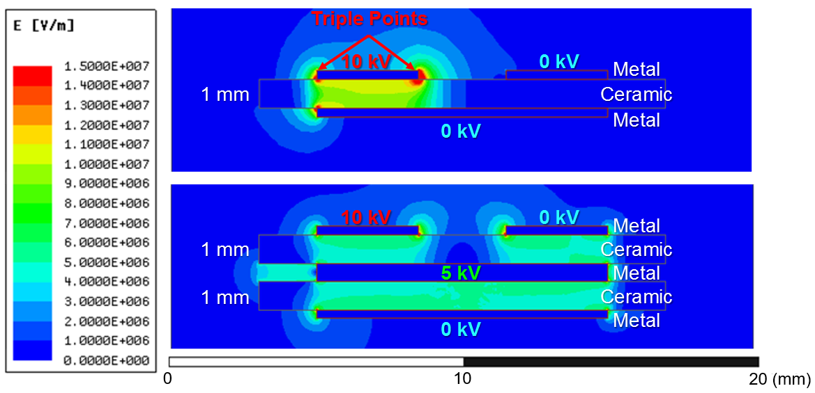
Fig. 1. Electric field of single (top) and stacked (bottom) substrates.
The gate- and power loop inductances of the designed module are each 9 nH (including the terminals), and the power density is 7.0 W/mm3. These low inductances and high power density were achieved by eliminating the antiparallel diodes and optimizing the substrate design and die and terminal arrangement. In order to address the enhanced electric fields associated with a high-voltage, high-density package, two direct-bonded aluminum (DBA) susbstrates are stacked on top of each other. By stacking two DBAs, the electric fields both within the ceramic and at the critical triple points, which, in this case, are where the aluminum-nitride, aluminum, and encapsulation meet, are drastically reduced. Fig. 1 shows a 2D electrostatic simulation conducted using ANSYS Maxwell. From the figure, the reduction in the peak electric field at the triple point can be clearly observed. Specifically, stacking two DBAs and connecting the middle metal layer to half of the applied voltage increased the partial discharge inception voltage by 63 percent. Due to the patterns and different potentials on the topside of the substrate, if the middle metal layer is left floating, then it may not drift to a potential that will result in a meaningful reduction in the peak electric field. Additionally, connecting the middle metal layer to the dc bus midpoint will reduce the common mode current that flows through the system ground since it creates a path for the current to flow back to the dc bus.
The fabricated 10 kV SiC MOSFET module is shown in Fig. 2. This module is made of semifunctional 10 kV SiC MOSFET die. This was done to test the fabrication processes and partial discharge without damaging the fully-functional devices. Once all of the tests have been completed and the processes have been optimized, the module will be constructed using the fully-functional 10 kV die.
Static characterization was performed on the fabricated module. The on-resistances are below the specified maximum value of 450 m?, and have a mild variation of 7 percent. The drain leakage current for the top switch is approximately 7 µA at 10 kV and 25o C. The bottom switch, on the other hand, has a breakdown voltage of 7.3 kV. Since these die were selected from a batch of semifunctional devices, it is not unlikely for them to have breakdown voltages below 10 kV. No partial discharge could be detected for the fabricated module up to 4 kV rms.
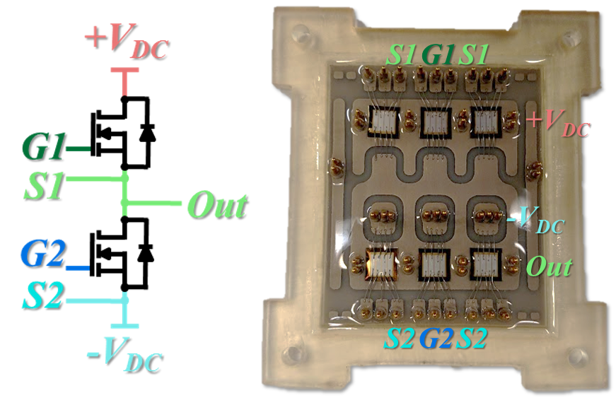
Fig. 2. Schematic and fabricated prototype module.
