LIBRARY
Development of Digital Control-Based Active Gate Driver for Stacked SiC MOSFETs

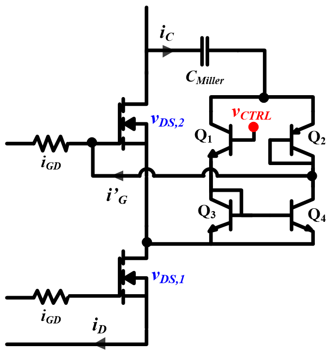
The bipolar junction transistor devices Q1 through Q4 in Fig. 1 serve as a current mirror network which adjusts the Miller current through the capacitor CMiller. The magnitude of the voltage signal VCTRL determines the magnitude of the Miller current directed to the device gate and the speed of the device at turn-off. Additionally, the Miller capacitance value affects the amount of current through Q1 and Q2, which also affects the drain-to-source voltage at VDS,2 in Fig. 1. Performing closed-loop feedback for the VCTRL signal with a digital controller holds several advantages over the use of an analog controller. Although voltage balancing within ±10 percent has been demonstrated with an analog proportional-integral (PI) technique, it took approximately six cycles (120 μs) to reach this voltage-balance range. By taking advantage of the ability to store memory with a digital processor, the initial condition of the controller can be stored for future iterations, which would prevent the delay in reaching a steady-state voltage balance during the first few cycles at start-up. Additionally, using a digital controller leads to a cost reduction and smaller footprint than the analog control implementation.
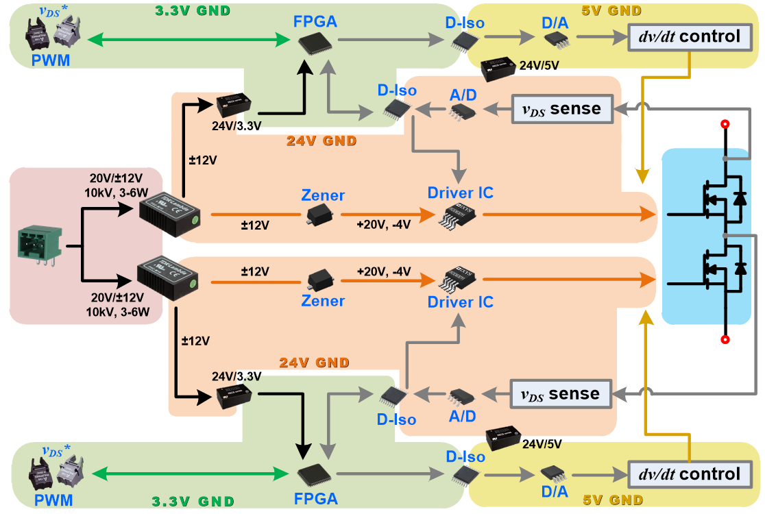
This paper focuses on the gate driver design process of the aforementioned voltage-balancing technique, using a digital controller. In particular, the design decisions for a processor chip and the feedback controller design are discussed. Short circuit and desaturation protection are also introduced, but continuous testing results with either technique are not included in this paper. Results for a double pulse test with a single 1.7 kV SiC MOSFET module are shown and compared against the same test setup performed with an analog controller


