


LIBRARY
Zero CMV Emission DC-DC Converter for UPS Application
Year: 2018 | Author: Paul Rankin | Paper: D5.1
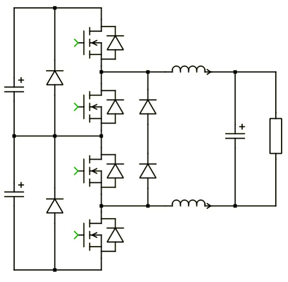
Fig. 1. 3-Level Buck Converter
The converter is based on a three-level topology common in inverter applications. A schematic of the topology is shown in Fig. 1. The converter works by synchronously switching two complementary pairs of switches to control power flow between the dc link and the battery backup, or vice versa. The upper switch and bottom switch operate synchronously and complementary to the upper, middle, and lower middle switches. In this way, the battery backup receives current symmetrically from the dc link capacitors, such that the common-mode voltage generation under ideal circumstances is zero.
Due to the characteristics of the SiC metal-oxide semiconductor field-effect transistors (MOSFETs) used in the converter, bidirectional power flow is achieved in excess of 99 percent efficiency up to the rated conditions of 20 kW. An efficiency curve is shown in Fig. 2 demonstrating the experimentally verified efficiency of the converter. Because of the wide bandgap technology, this topology is still more efficient than many traditional Si buck converters, despite having twice as many devices in order to reduce the overall EMI profile. Additionally, the converter is able to provide some control functionality to the system due to an ability to asymmetrically transfer power from the DC link to the battery. Therefore, at the cost of an increased common-mode voltage profile, the converter can maintain a balanced dc bus voltage during operation.
Finally, through simulation and experimental results, this topology shows some benefit concerning the impact on the overall noise profile of the system while operating. When compared to a traditional buck converter, the simulated improvement in the overall noise profile of the converter is up to 14 dB. Experimental results show a similaralthough not as drasticimprovement. This reduced noise profile, combined with the high efficiency previously shown, is the main reason this topology should be considered for commercial UPS applications. In addition, since the topology is the same as that of a three-level inverter/rectifier, design for manufacturing systems using this topology is improved by the nature of shared components such as gate drivers and device footprints. In conclusion, such a topology, when combined with wide bandgap technologies, shows a number of marked improvements compared to existing solutions.
