LIBRARY
Electromagnetic Interference Reduction Techniques for Gate Driver Design of Medium-Voltage SiC MOSFET

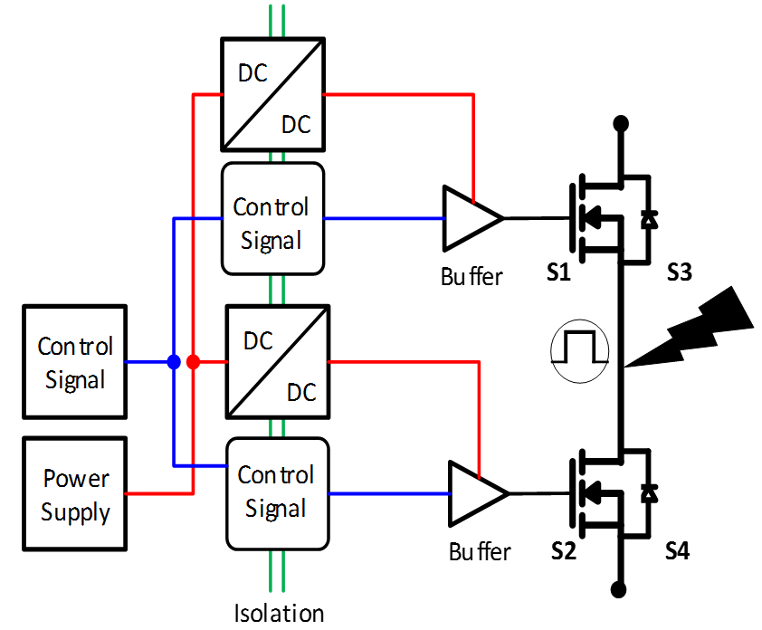
A fast switching transition (dV/dt) is preferred to achieve lower switching loss, and hence higher efficiency. However, this comes at the expense of conducted and radiated electromagnetic interference (EMI). A high dV/dt can cause severe EMI current disturbances at the middle point of the phase leg, as shown in Fig. 1. It is important to address and mitigate such disturbances using proper techniques, and without underutilizing the maximum capability of the device's switching speed. Absent careful consideration and attenuation of the common mode current,vexcessive stress on the gate driver can result, making both the fidelity of the control signal and operation reliability difficult to improve.
The proposed gate driver architecture overcomes the EMI disturbances by changing the current paths, mostly on the high side. It is important to separate the noisy currents from the control signal. By introducing a higher impedance path in the high side on both the power loop and the signal loop, the perturbations caused by the high frequency current on the control of the drivers can be minimized.
In this paper, EMI noise propagation paths are analzyed during a fast switching transition. The simulation results support the claimed advatange of the gate driver immunity to the EMI disturbances under very high dV/dt).


