


LIBRARY
Design, Characteristics, and Application of Pluggable Low-Inductance Switching Power Cell of Paralleled GaN HEMTs
Year: 2018 | Author: Bingyao Sun | Paper: T1.1
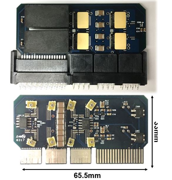
Fig. 1. Top (upper) and back (lower) side of the switching cell design of two GaN HEMTs paralleled.
This paper proposes solutions for paralleling two or four GaN high-electron-mobility transistors (HEMTs) with a 1 Ω gate resistor. The gate loop inductances of the paralleled devices are minimized to 2.4 nH with 0.1 nH difference. The power loop inductance is also minimized to 3 nH with a footprint of 65.5 mm × 33 mm. Based on the proposed design shown in Fig. 1, the double-pulse test is performed with 400 Vdc, 100 A load current with 1 Ω gate resistance. The small gate resistance enables very fast turn-on and turn-off speeds with minor oscillation on the gates, as shown in Fig. 2. Furthermore, an adaptive thermal solution is proposed, which offers a customized heat sink to control the air flow and fully utilize the space. The commutation between the two paralleled devices during turn-on, where a very large gate oscillation occurs, is explained based on the experimental waveforms. It is found that the combination of gate resistor values has a significant impact on gate oscillation when two devices are paralleling. The switching losses with different turn-on and turn-off gate resistors are measured and compared. Finally, the designed switching cells are tested in a 400 V input voltage, 10 kW output power LLC resonant converter switching with up to 450 kHz switching frequency. This example illustrates how the switching cell can be utilized to build a high efficiency (98 percent) and high power density (131 W/in3) converter for battery charger applications.
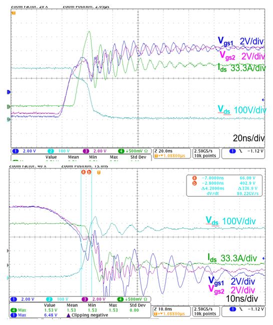
Fig. 2. Double pulse test waveforms with Vdc= 400 V, Ids = 100 A, Rg = 1 Ω: upper: turn-on, lower: turn-off.
