


LIBRARY
Analysis and Design of an Overcurrent Protection Scheme Based on Parasitic Inductance of SiC MOSFET Power Module
Year: 2018 | Author: Keyao Sun | Paper: T3.4

Fig. 1. Overcurrent detection circuit.
Fig. 2 below (RsCs = 3e-6 to guarantee the linearity) shows the test result of drain current id and output voltage -vo. In order to show the matching between vo and id, vo is flipped here to positive. It is clear that the output voltage -vo nicely describes the drain current id during the rising edge. From the test result, the current value is around 1000 times the output voltage, so the parasitic inductance can be calculated.
The designed circuit includes two branches, which can not only detect an intense short circuit fault within 80 ns, but also detect a relatively slow overcurrent that could generate excessive heat and damage the system. The proposed scheme uses only a few simple and cheap components compared to other methods, and does not require any special techniques in a printed circuit board (PCB) (e.g., a Rogowski coil), or during the manufacture of the module (e.g., a current mirror). Other advantages of the proposed method include a lack of temperature dependency, wide sensing bandwidth and current range, very fast response speed, and high sensor density. A gate driver with embedded overcurrent protection is designed with a small profile (90 mm * 65 mm * 8 mm) and wide operation temperature range up to 105 °C.
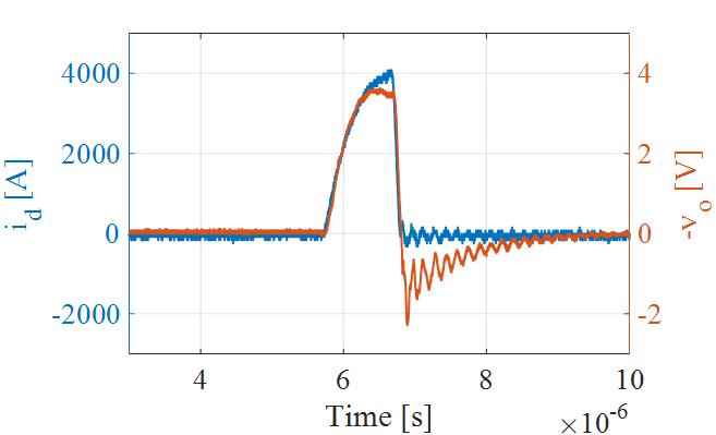
Fig. 2. Short circuit current and detection voltage signal
