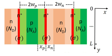
Fig.1. Schematics of superjunction with interface charges
Achieving high breakdown voltage with low specific-on resistance is one of the main objectives for power devices. Vertical superjunction devices could break the theoretical limit of unipolar power devices, by allowing linear design dependence of specific-on resistance with breakdown voltage. Si superjunction devices have achieved huge commercial success. The presence of interface charge at the regrown surface is a key roadblock for experimental realization of GaN superjunction devices. However, analytical modeling for superjunctions with interface charges remains undone. This work studies the numerical model for superjunctions with interface charges, including GaN superjunctions as a case study. The specific-on resistance vs. breakdown voltage relationship is assessed together with the optimizing strategy for doping and geometry. The interface charge that exists between n-pillar and p-pillar is shown in Fig.1. The existence of an interface charge will affect the charge equilibrium and electric field continuity on the interface, thus the depletion width inside n-pillar will be affected by the interface charge. Since on-state current only flows in n-pillar, the minimum depletion width will give maximum conductivity. This means on resistance
Ron is a function of the interface charge. Another crucial parameter is the breakdown voltage
VB. At breakdown, the lateral electric field amplitude is dependent on interface charge. Assuming the total critical electric field is constant, then the vertical electric field at breakdown will also be affected by interface charge. This vertical electric field will directly contribute to the breakdown voltage. Both the analytical equations are given for specific-on resistance
Ron and breakdown voltage
VB. The figure of merit,
Ron/
VB , can be deduced and its minimum point can be achieved by optimizing doping concentration
ND and n-pillar width
wn, as shown in Fig. 2. The material properties of GaN are considered in this model for design optimization, and are compared with the no-interface charge case. The optimized result shows similar behavior compared with no-interface charge results. In fact, the difference is almost negligible when the width is not too small (>1 μm) . All of them show advantage over unipolar devices at high voltage (>1000 V). In conclusion, this work provides the first analytical model for understanding superjunction devices with interface charges. The case study of GaN superjunctions reveals promising features of vertical GaN superjunction devices. Though not as ideal as no-interface charge cases, problems can be greatly compensated for by optimizing doping concentration and pillar width. This work will remove the roadblocks of experimental demonstration of vertical GaN superjunctions.
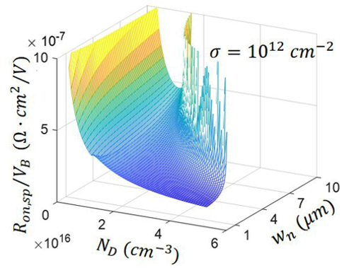
Fig. 2. Optimization of R_(on,sp)/V_B for variable doping concentration and width.


