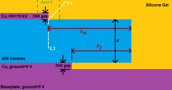
Fig. 1. Geometries considered for simulations
Silicon carbide (SiC) and gallium nitride (GaN), which have a relatively large bandgap of 3.3 eV and 3.4 eV, respectively, are the more promising semiconductor materials known as wide bandgap (WBG) semiconductors. This is due to their outstanding properties such as commercial availability of starting material and maturity of the technological processes. WBG semiconductors, which are expected to have better efficiency, higher temperature tolerance, and higher voltage blocking capability than their silicon (Si) counterparts having a bandgap of 1.1 eV, are changing the landscape of the power electronics industry. Moreover, a new class of semiconductor materials called ultrawide-bandgap (UWBG) semiconductors, with bandgaps higher than that of GaN, including currently investigated diamond (C), gallium oxide (Ga
2O
3), and aluminum nitride (AlN), will be the generation-after-next power electronics. However, new packaging technologies are needed to realize the afore mentioned superior system performance with WBG and UWBG devices. Among the various factors needing to be addressed for high-density packaging designs of high voltage WBG and UWBG devices, are the high electric fields, especially at the edges of the substrate metallization. These can lead to unacceptable levels of partial discharges in the silicone gel, commonly used as encapsulations. In this paper, geometrical techniques for electric field control inside WBG power electronics modules are studied by finite element method models (FEM), developed in COMSOL Multiphysics. Fig. 1 shows the geometry considered for modeling in COMSOL Multiphysics. The upper and lower copper metallization thickness is 300 ?m which is a common value for ceramic substrates. The following were considered: the relative permittivity values of 8.9 and 2.7 for AlN and silicone gel, respectively; and the voltages of 10 kV addressing the blocking voltage of a WBG device for the upper metal layer, and 0 for the lower metal layers. As shown in Fig. 2, an offset of the two metallization layers is defined as r
off&equalsr
u-r
l for r
u and r
l. Fig. 2 shows the electric field magnitude values at a distance of 20 ?m from the edge along the dashed line L1, shown in Fig. 1, for different values of r
off for a 630 µm ceramic layer. It is apparent that with decreasing the offset, the electric field magnitude reduces. Stated simply, an increase in the length of the upper metal layer, relieves the worst high field region. This is due to the influence of the grounded based plate; the longer the upper metal layer, the less nonuniform the electric field. Changing r
off from 0.35 mm to -0.5 mm reduces the electric field intensity up to 57 % and becomes an efficient electric field control technique.
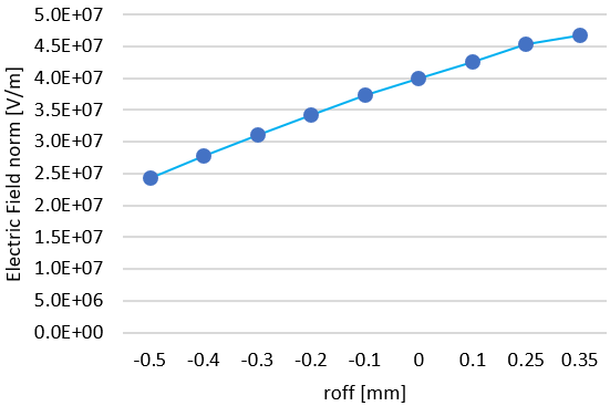
Fig. 2. Influence of roff on electric field intensity


