LIBRARY
The Optimal Design of A High-Temperature PCB-Embedded Transformer GaN-Based Gate-Drive Power Supply with A Wide-Input Range

Since working conditions change with input voltage, the circuit design and the transformer design become difficult. At low voltag- es, the conduction loss of the primary devices dominates due to the higher current. As the input voltage increases, the reverse-recovery loss of the rectifier diodes plays the leading role. Apart from the operating mode selection, the design freedom of the transformer is limited. Described in Fig. 2, the transformer design is restricted by the controller duty cycle range and zero-voltage switching (ZVS) requirement, which are represented by the red and blue curve, respec- tively. Failing to meet these requirements leads to either insufficient voltage gain or low efficiency.
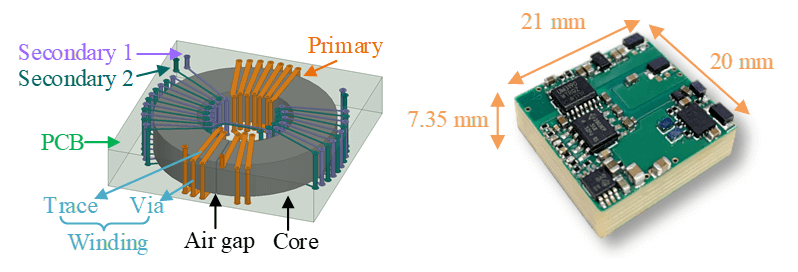
In this paper, a GDPS with two isolated outputs of 24 V is designed. Its input voltage ranges from 8.5 V to 28 V, and the power rating of each output is 5 W. The size is 21 mm × 20 mm × 7.35 mm, representing a power density of 53.2 W/in3. To design the targeted GDPS, this paper first presents the design approach and optimized results, including the circuit design and transformer optimization, after which the current and voltage information can be estimated and used for selecting the conponents. Layout design, hardware as- sembly, and the evaluaton of the proposed GDPS are then provided. The permeablity degradation issue of the PCB-embedded transformer caused by mechanical stress during fabrication is revealed in the end of this paper.


