LIBRARY
Commutation Loop Analysis and Optimization for a SiC- Based 25 kW, 380:460 V Three-Phase Matrix Converter
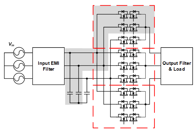
Overlapping power traces cause magnetic flux cancellation, which in turn reduces overall loop inductance. This gain is limited by the presence of parasitic capacitances induced by the interaction of jumping nodes. Trade-offs between these factors must be considered when designing the layout of the PCB. Thermal management must also be assessed in the layout of the commutation loops, as certain strategies inform constraints on the design. In this paper, various cooling methods are discussed and evaluated. Thermal vias and a ceramic inlay are two techniques that both meet the requirements needed for this application. Power loop layouts of a single-phase leg are then completed for these cases.
The new phase leg layouts (P2 inlay, and P2 thermal via) are compared to an existing layout, P1, using finite element analysis (FEA) to extract the loop parasitics. These are then used to perform a double pulse test simulation. A sample of the results are displayed in Fig. 2. The lower commutation loop inductances produce lower peak voltages, and less ringing in the switching transients.
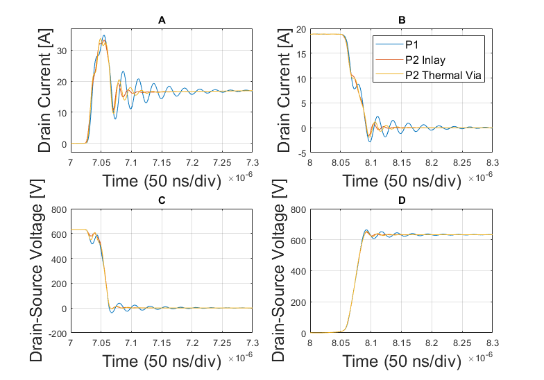
(b) turn-off and drain-source voltage, (c) turn-on, and (d) turn-off.


