


LIBRARY
Superjunction Power Transistors with Interface Charges: A Case Study for GaN
Year: 2020 | Author: Yunwei Ma | Paper: T1.12
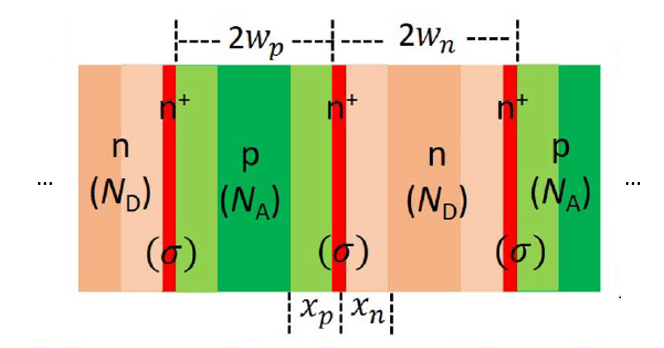
Fig. 1. Illustration of n-pillars and p-pillars with interface charge
Recent progress in p-GaN trench-filling epitaxy has shown promise for the demonstration of GaN SJ devices. However, the presence of n-type interface charges at the regrowth interfaces has been widely observed. Fig. 1 is an illustration of the SJ structure with an interface charge. These interface charges pose great challenges to the design and performance evaluation of SJ devices.
This work demonstrates an analytical model for SJ devices with interface charges for the first time; the model is derived from an electrostatic equation. This analytical model provides important design guidelines to minimize the adverse impacts induced by interface charges on SJ performance. Two different design guidelines were quantitatively investigated for GaN SJ devices, one to adjust doping concentration and the other to adjust geometry. The doping modulation was identified to be a superior approach to compensate interface charges. The TCAD simulation of vertical GaN SJ transis- tors validated our analytical model, as shown in Fig. 2. With opti- mal designs, vertical GaN SJ transistors with interface charges retain great advantages over the conventional GaN power transistors, while their design windows are smaller compared to ideal GaN SJ devices. This work provides important design guidelines for a verti- cal GaN SJ devices demonstration.
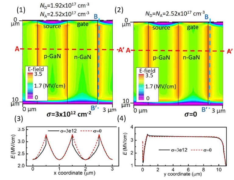
Fig .2. (a) Electrical field distribution of SJ with interface charge; (b) electrical field distribution of SJ without interface charge; (c) electrical field along A direction; and (d) electrical field along B direction
