


LIBRARY
16kV Input 200kW Rated SiC Based Three Phase Inverter
Year: 2020 | Author: Lakshmi Ravi | Paper: T1.16
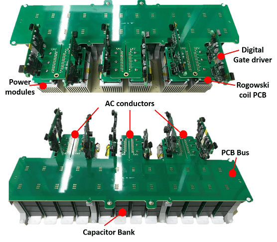
Fig. 1. 16 kV input, 200 kW rated three-phase, two-level inverter assembly using Wolfspeed 10 kV, 16 A SiC modules
In this work, a three-phase, two-level inverter rated for 200 kW, 11 kV ac output fed by a 16 kV dc input is realized using a two-level topology with two series-connected 10 kV SiC MOSFETs per switch position. All inverter components including the gate driver, Rogowski current sensor, MV modular planar PCB bus, power quality filter and forced air thermal management system are designed with considerations for the high operating voltage. The full inverter system is shown in Fig. 1.
Apart from the basic driving features, the designed gate driver is equipped with an active voltage balancing capability to guaran- tee that the turn-off voltage is equally shared between the series- connected MOSFETs. The Rogowski-sensor-based shortcircuit protection ensures synchronized fault protection with a reaction time < 500 ns. The MV PCB-bus and capacitor bank are designed for partial-discharge-free operation up to 18 kV and help integrate all system components into a single high power density assembly. The thermal management system uses forced air cooling to keep the maximum device junction temperature below limits. The power quality filter components are designed to meet IEEE 519 harmonic standards with necessary insulation to withstand high dv/dt.
All the designed components are tested individually for func- tionality and insulation withstand before system assembly. The final inverter is tested in a three-phase, continuous pump-back test in open loop with a specially designed isolated 16 kV dc supply and reactive load. The phase difference between voltage references of each phase is reduced so that the resulting voltage on each inductor can be kept at a low value. This way the modulation index does not need to be reduced to a very small value to operate at the rated output current of 10.5 A rms. The inverter output waveforms at the 16 kV dc-bus is shown in Fig. 2.
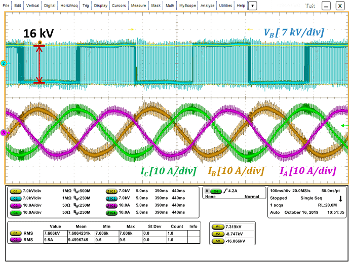
Fig. 2. Inverter output voltage and three-phase currents at 16 kV dc bus, 10.5 A rms
