


LIBRARY
PCB Winding Coupled Inductor Design for Critical-Mode-Based Three-Phase Bidirectional AC-DC Converters with Balance Technique
Year: 2020 | Author: Zhengrong Huang | Paper: T2.4
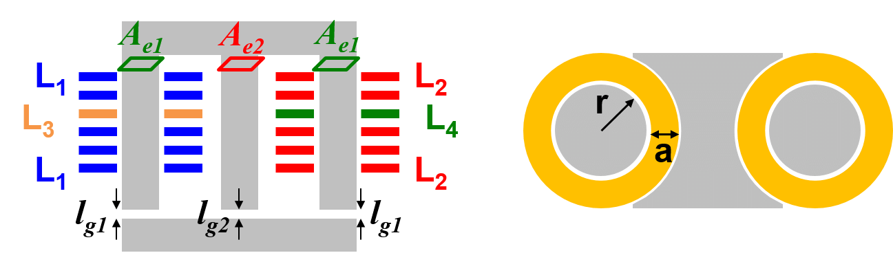
Fig. 1. PCB winding inductor structure and cross section view.
Based on the three-phase ac-dc circuit topology with balance inductors, EI core structure is selected for the coupled inductor in each phase, which is shown in Fig. 1 with an example of a 6-layer inductor. The cross section view of the EI core structure is also shown in Fig. 1. In order to design these PCB winding coupled inductors, the required inductance needs to be determined in order to achieved the target switching frequency design. Therefore, in this work, first an analytical operational model is developed to determine the required self inductance and mutual inductance. With the reluctance model, the required reluctance can be determined. Then, based on the circuit simulation, the flux in the magnetic core can be calculated.
After that, the outer leg radius r and the winding width a are defined as two independent design variables. By sweeping these two design variables, the inductor loss and inductor footprint can be calculated. At each inductor footprint, there is one design point with minimum inductor loss. By combining all these design points, the optimal design curve is obtained and shown in Fig. 2. On this curve, a design point is selected around the knee area, as the star shows in Fig. 2. The loss and the footprint at the selected design point are similar compared with the results of the litz-wire based coupled inductor, and therefore similar efficiency is expected with the PCB winding coupled inductor design.
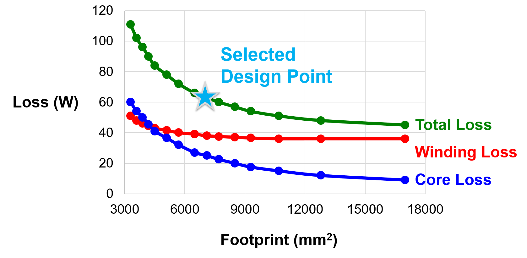
Fig. 2. Optimal design curve of a PCB winding coupled inductor.
