


LIBRARY
A High-Efficiency High-Density Wide-Bandgap Device-Based Bidirectional On-Board Charger
Year: 2020 | Author: Rimon Gadelrab | Paper: T3.4
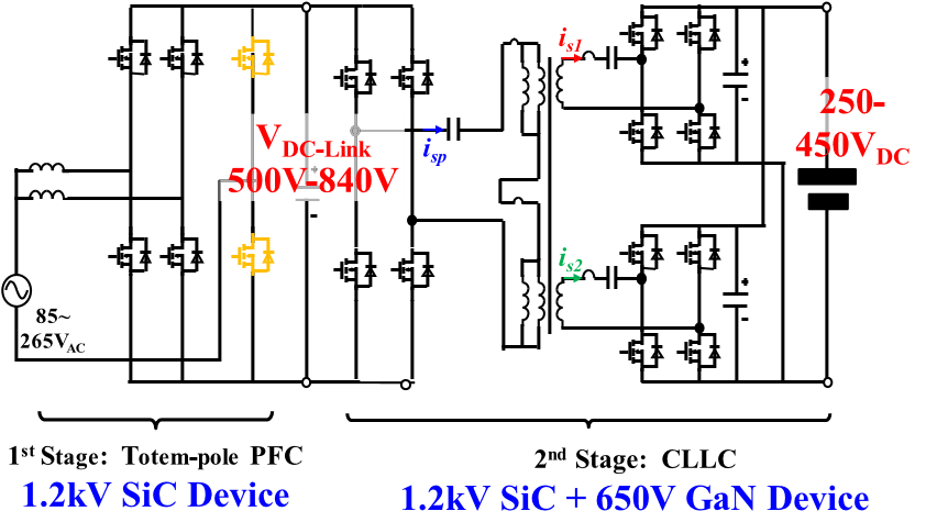
Fig. 1. Variable dc-link voltage structure without split capacitors.
For the ac-dc stage, a bridgeless totem-pole converter with CRM operation is adopted. Zero voltage switching (ZVS) is achieved for all fast switches, making it a promising candidate for high-frequency operation. Also, the symmetrical structure guarantees easy bidirectional operation. For the isolated dc-dc stage, the CLLC resonant converter featuring the same soft-switching technique as the LLC resonant converter is selected. It achieves ZVS for all switches under all load conditions. In addition, the symmetrical resonant tank makes it much more suitable for bidirectional operation. To optimize the converter over a wide output voltage range, a variable dc-link voltage structure is used, utilizing 1.2-kV SiC devices so that the second stage CLLC resonant converter is always working around its optimized point for all output voltages. As a result, very high efficiency is achieved during the whole charging cycle, from low battery voltage to high battery voltage. Also, a two-stage combined control strategy is proposed for both charging and discharging operations. The proposed control guarantees that the dc-dc stage switching frequency stays around resonant frequency and also eliminates the secondary order line-frequency ripple generated by the ac-dc stage. A 6.6 kW, 500 kHz (300 kHz for ac/dc) bidirectional on-board charger prototype with 37 W/in3 power density and over 96% efficiency is demonstrated to verify the proposed structure.
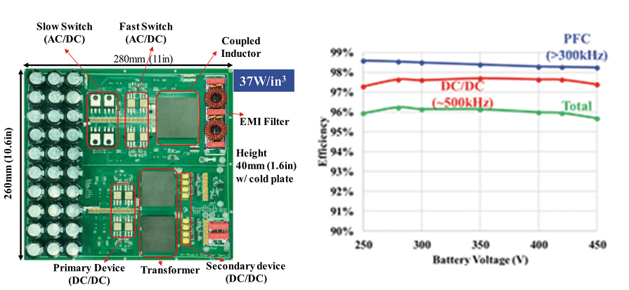
Fig. 2: The hardware prototype and tested efficiency.
