


LIBRARY
Operation and Control of Converters Having Integrated Capacitor Blocked Transistor Cells
Year: 2020 | Author: Jianghui Yu | Paper: T4.18

Fig. 1. Dc-dc boost converter with ICBT cells.
voltage ripples small, the internal capacitors are usually large.
Integrated capacitor blocked transistor (ICBT) cells provide an alternative solution. Fig. 1 shows a dc-dc boost converter built with ICBT cells. There are two cells per converter arm. Each cell consists of a pair of complementary switches and a cell capacitor. When the bottom switch is on, the output voltage is zero; when the top switch is on, the output current reduces to zero quickly. The two switching states are similar to a single device. The total semiconductor loss of one cell is also similar to a single device. Electric power is directly transferred through the ICBT cells during their on state. Therefore, much smaller cell capacitance is required compared to cell capacitors in MMCs. The cells in the same arm operate synchronously and be- have like a single high-voltage device. Converters having ICBT cells have voltage scalability like MMCs, and ICBT cells can be used to build converters with different topologies.
The voltage each device blocks is the voltage of the corresponding cell capacitor, which is half of the dc-bus voltage in this case. Voltage balancing is achieved when the cell capacitor voltages are well controlled. Ideally, all the cells in one arm switch at the same time and with the same speed so that all the cell capacitors share the same current and the voltage. However, the switches always have different switching timing and speed because of parameter mis- matches and parasitics. Voltage differences may accumulate among the cell capacitors and must be controlled. Fig. 2 (a) shows the two lower arm cell capacitor voltages during 20 switching cycles. It is assumed that all the switching devices are the same, but 20 pF parasitic capacitors exist from all device gate terminals and drain terminals to the ground. Because of the high dv/dt across the parasitic capacitors, the bottom devices in two lower arm cells have different gate currents and different drain currents, causing different switching speeds. As a result, two capacitors have different currents, then different voltages. The first cell capacitor voltage (in green) has a lower value than the second cell capacitor voltage (in blue). The capacitor voltage control is realized by adding proper delays to the gating signals. Fig. 2(b) shows the two lower arm cell capacitor voltages with the control. Reference gating signals are generated by the converter level control and sent to each arm. Then each cell makes its own decision whether to add delays based on sensed cell capacitor voltage and arm current. In this case, the turn-off action of the second cell is delayed so that the second cell capacitor is charged for less duration. The two capacitor voltages remain the same. This control works the same way when there are more cells.
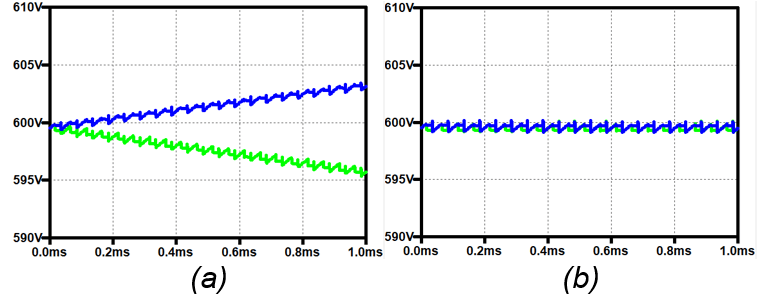
Fig. 2. Lower arm cell capacitor voltages (a) without control and (b) with control.
