LIBRARY
Design of a PCB-based Laminated Bus for 10 kV SiC MOSFET-based Converters
In this work, a low inductance PCB-based bus is designed to support Wolfspeeds XHV-6 series 10 kV SiC MOSFET module.
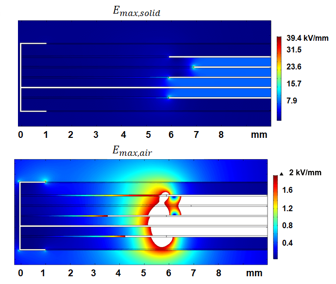
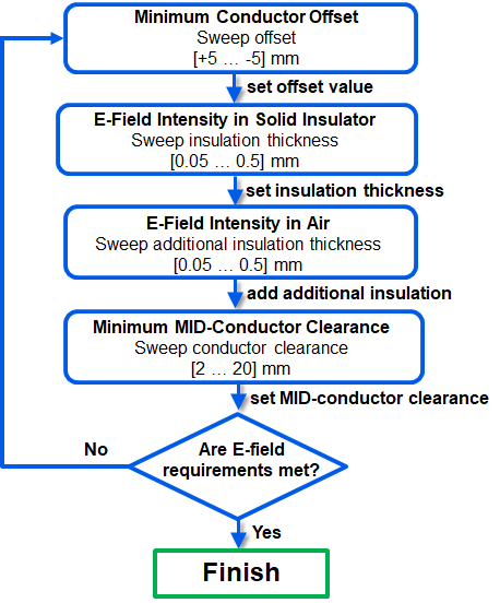
The E-field was analyzed in high intensity regions using COMSOL for finite element analysis (FEA). A midpoint layer separating the +/- dc layers was implemented to reduce the peak intensity near the insulator/connector interface. Geometric techniques for field control along the surface and within the PCB were implemented us- ing the design flow shown in Fig. 1. The results for the final E-field intensity after completion of the design flow are shown in Fig. 2. It should be noted that the field in air is of interest in the bottom image in Fig. 2; therefore, data above 2 kV/mm has been restricted and ap- pears white within the PCB dielectric. Simulation results show that the peak E-field intensity can be reduced by adding a slight offset between conductors at a different potential. Due to the voltages of interest, the E-field intensity in air was most efficiently controlled by forcing the field in an additional dielectric layer placed on the outside of what would normally be the outermost power plane.
The design criteria determined from simulation were implemented in a PCB. Multiple conductors were paralleled to increase the current-handling capability and improve current distribution among in-pad vias. PD tests showed the bus to be PD- and corona- free up to 11.52 kV. High current density regions at the bus remained below 70° C with 85 A output, making it suitable for a 6 kV, 500 kW converter.
