LIBRARY
Auxiliary Power Network Architecture for 10 kV SiC-based Power Electronics Building Blocks

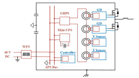
Fig. 1 shows the proposed auxiliary power network architec- ture of one power electronics building block (PEBB). The black part in Fig. 1 shows the main power components of the 10 kV SiC MOS- FET-based PEBB, including SiC MOSFETs, load inductor and dc- link capacitors. The blue part shows all the possible loads, including controller, gate drivers, voltage sensor and temperature sensor (the current sensor is the Rogowski coil embedded in the gate driver), that require power from the APS network. The red part shows the APS network components, including the two-stage solution with a mini-UPS as backup power. The first stage is the WPT getting power externally. The second stage is the current-transformer-based GDPS fed from the WPT.
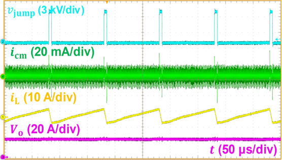
Fig. 2 shows the test results of the two-stage power supply in a medium voltage 6 kV buck test. In this test, the WPT gains power from a benchtop power supply, so the reference point of the sending side for the WPT connects to the ground potential, and the reference point of the receiving side as well as the sending side of the GDPS connect to the midpoint of the bus bar, as discussed above. The gate driver for the top switch is powered by the WPT and GDPS, and the bottom gate driver is powered by a commercial isolated power supply. The switching node voltage Vjump, inductor current IL, common mode current out of GDPS I


