LIBRARY
Voltage Balancing of Four Series-Connected SiC MOSFETs under 2 kV Bus Voltage using Active dv/dt Control
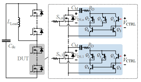
In reference to Fig. 1, the current mirror network regulates the flow of the current injected by the additional capacitor CM. This capacitor CM injects a current dependent on the individual dv/dt rate seen at each drain that slows down the switching transition of the MOSFET in question. The VCTRL signal is then used to adjust the amount of current flowing back to the gate, acting as an additional linear Miller capacitance, or flowing to the source of the device di- rectly and bypassing the gate terminal. With Q1 off, all the current flows to the gate for maximum effect, slowing down the power MOSFET. By increasing the current through Q1 gradually, the slow-down effect will be reduced. Each control voltage parameter VCTRL across Q1 determines the magnitude of current injected at each device gate.
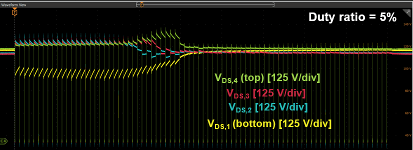
Fig. 2 shows the experimental results for four MOSFETs under test with a 2 kV dc bus, where all devices block approximately 500 V each in steady-state after closed-loop compensation. One contribution of steady-state error can be attributed to the use of potentiometers for the reference voltage of each separate gate-driver, which can have small tolerance differences.
