LIBRARY
Medium Voltage PCB-based DC Bus Design Considering Current Handling Capability

A PCB-based bus was implemented utilizing geometric techniques for a well-controlled E-field. The manufacturing process provides less defects allowing the bus thickness to be reduced by approximately 75% compared to the traditional laminated while increasing the PDIV from 5.6 kV to 10.5 kV. Multiple parallel layers were used for +dc and -dc to allow a current handling capability of at least 85 A.
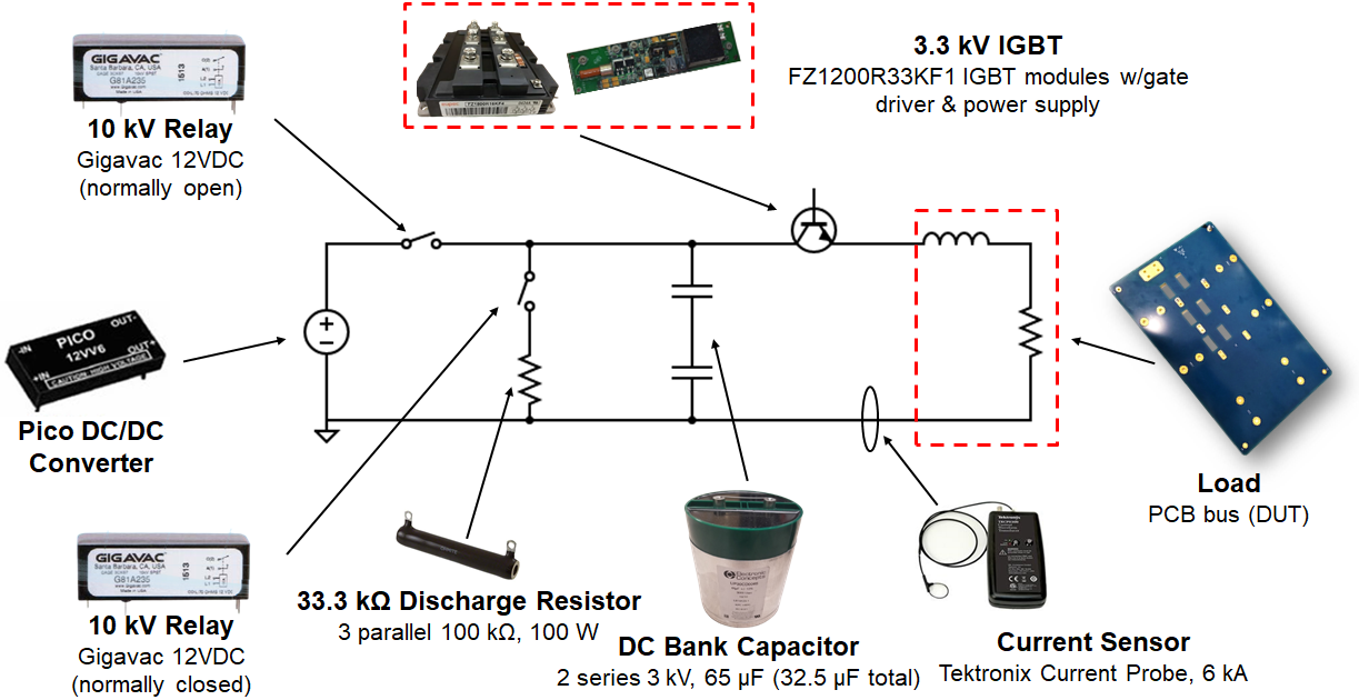
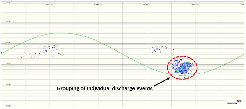
During short circuit (SC) fault events, a high peak current can create a large force on the conductors, especially in high current density areas. This force can effectively peel the copper from the dielectric; thus, voids are introduced and the PDIV is decreased. A SC testbed has been constructed to allow SC testing up to 4500 Apk; see Fig. 1. A new bus is used to determine the initial PDIV and the phase resolved PD pattern (PRPD) is recorded as shown in Fig. 2. Repetitive SC events are generated with 20 seconds between pulses to allow capacitor recharging and ensure no degradation is caused from copper self-heating. Every 20 SC events, the PDIV is checked and PRPD recorded to aid in identifying insulation degradation. This work will be used to further improve the layout of PCB-based buses to ensure the long-term reliability.


