LIBRARY
Design of Three-level Flying-capacitor Commutation Cells with Four Paralleled 650V/60A GaN HEMTs
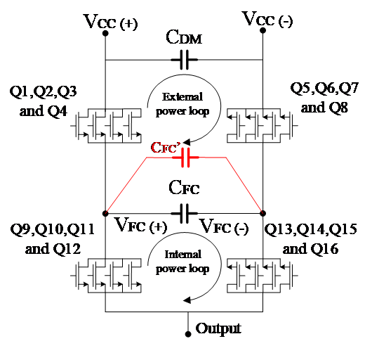
Each leg of the three-level FC inverter is composed of 16 semiconductors as shown in Fig. 1. Different PCB designs were considered using simulation in Ansys Q3D Extractor to define the solutions with lowest power loop inductances given layer symmetry, differential mode (CDM) capacitors, and FC (CFC and CFC'/CFC'') ceramic capacitors positioning. In both versions, gate driver circuit, power connector, and the four paralleled GaN HEMTs have the same disposition: two transistors on top layer and two on bottom layer. Beyond the PCB layers routing, ceramic capacitors positioning is the key point to optimize power loop stray inductances, especially for CFC that influences both external and internal power loops shown in Fig. 1.
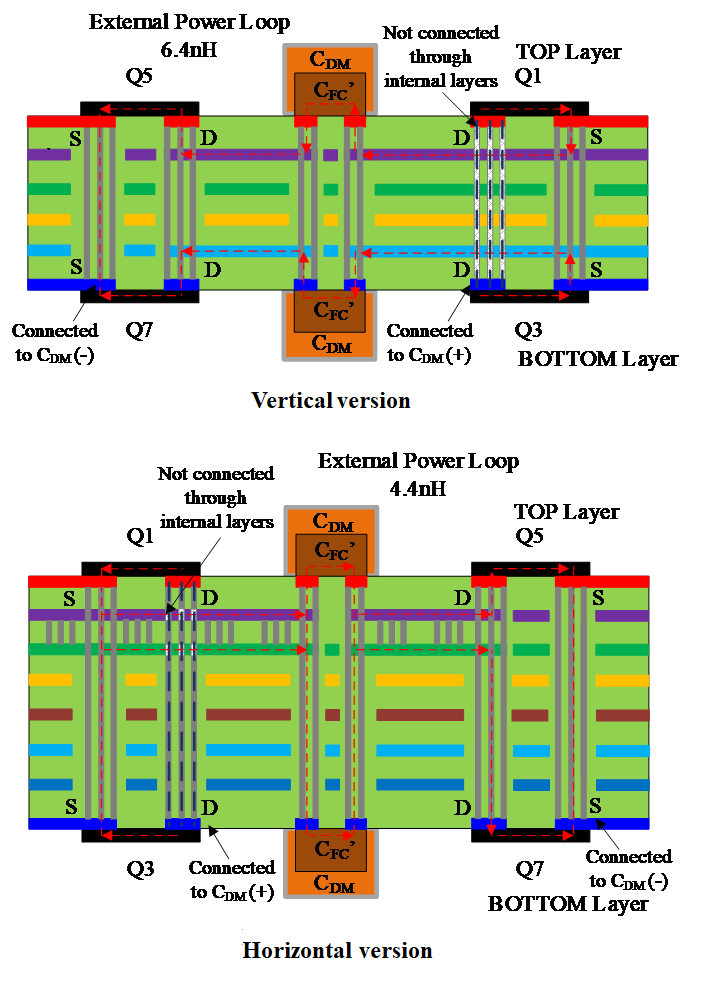
Fig. 2 presents the side view of the power loop of different versions. Vertical version presents more symmetry disposition of layers (6 layers) and 6.4 nH and 5.7 nH of external and internal power loop inductances, respectively. The Horizontal version presents a dissymmetry regarding top and bottom paralleled devices and PCB layers. It has 8 layers but has only 4.4 nH and 3.6 nH for external and internal loop stray inductances. This inductance reduction compared to the Vertical version is due to CFC'' (which is an extra CFC). The Horizontal version routing allows an easy way to cascade flying-capacitors cells in series to increase inverter output voltage levels. The Horizontal version presents lower loop inductances at the expense of thicker PCB layers and asymmetry between top and bottom paralleled devices. From the test results of the Vertical version, overvoltage of both internal and external loops are below 10%.
