RESEARCH
Solution for efficiency limitation imposed by input decoupling capacitor in non-isolated DC/DC converters (2004)

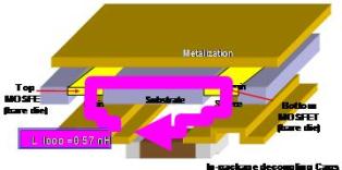
Using a novel system design method called Stacked Power where unpackaged devices (IR DirectFETs in this case) are embedded inside a layer of aluminum nitride ceramic, the impact of this problem has been minimized. This arrangement allows for a flush top and bottom mounting so that the decoupling capacitor can be placed directly on top of the devices, effectively creating the smallest possible loop. Maxwell 3D simulations show that this design yields a 0.8nH loop inductance, which is the lowest achievable with conventional 20V devices and a 0805 ceramic capacitor since they physically cannot be closer together.
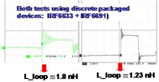
Figure 1 shows that moving the capacitor closer to the devices reduces the parasitic ringing at the switch node considerably. Even a 0.6nH inductance reduction has a significant impact. Figure 2 shows the Stacked Power module with the decoupling capacitor directly on top of the embedded switches.
This concept was demonstrated by CPES in February of 2007 and has since been adopted by Hitachi research group for use with their DrMOS, as shown at APEC in April 2008 by Dr. Hashimoto.


