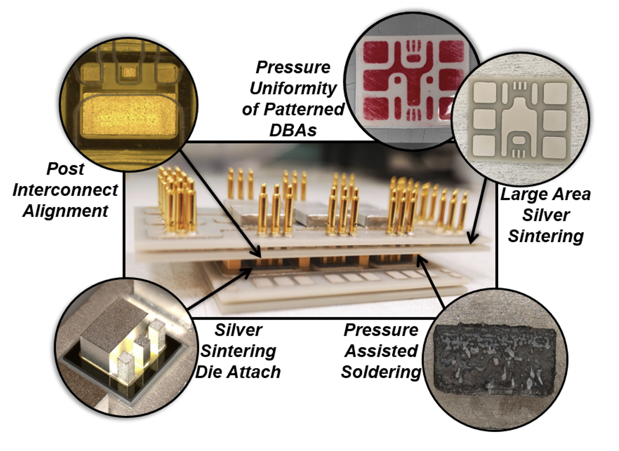
Fig.1. Fabrication refinements for multi-chip power modules.
Improvements in packaging technologies have increased SiC power modules' operation to 10 kV through the advancement of low-inductance designs and electrical insulation techniques. Post interconnects attached to stacked substrates using silver sintering enable these low-inductance, power-dense modules that allow for double-sided cooling. Machined post interconnects have height variances, which become more problematic as the number of posts increases with the number of dies in parallel for multi-chip power modules (MCPMs). Silver sinter paste is a solid-solid diffusion process; thus, defects that occur during application remain in the bond line. These fabrication challenges can reduce bond quality in the power and signal loops, resulting in a low yield of functional modules. The fabrication refinements illustrated in Fig. 1 will improve the yield of MCPMs. These refinements are demonstrated through successfully fabricating the MCPM in Fig. 1 using the National Institute of Advanced Industrial Science and Technology's (AIST) 13kV, 705mΩ silicon-carbide (SiC) metal-oxide semiconductor field-effect transistors (MOSFETs).
Implementation of the refinements resulted in low-resistance solder bonds, planar die-attached sinter bonds, uniformly sintered substrates without warpage or cracking, and reliable connections from the substrate to the post-interconnects across every device in the MCPM. Due to the limited availability of 13kV die, a module with one die per switch position was first fabricated and characterized to verify these refinements. Fig. 2 shows waveforms during a 2.2kV, 5A double-pulse test (DPT). Even at a voltage lower than the device's maximum, initial testing shows successful fabrication by stressing the maximum device current with no bond failures. The drain-source voltage has an overshoot of 3%, achieved due to the low parasitic inductance offered by the post-interconnect module structure. The drain-source voltage rise and fall times are 130 ns and 30 ns, respectively, with a maximum dv/dt of 62 V/ns at 2.2 kV, 5 A.


