


LIBRARY
Gate Switching Robustness and Reliability of GaN P-Gate HEMTs
Year: 2023 | Author: Bixuan Wang | Paper: H1.5
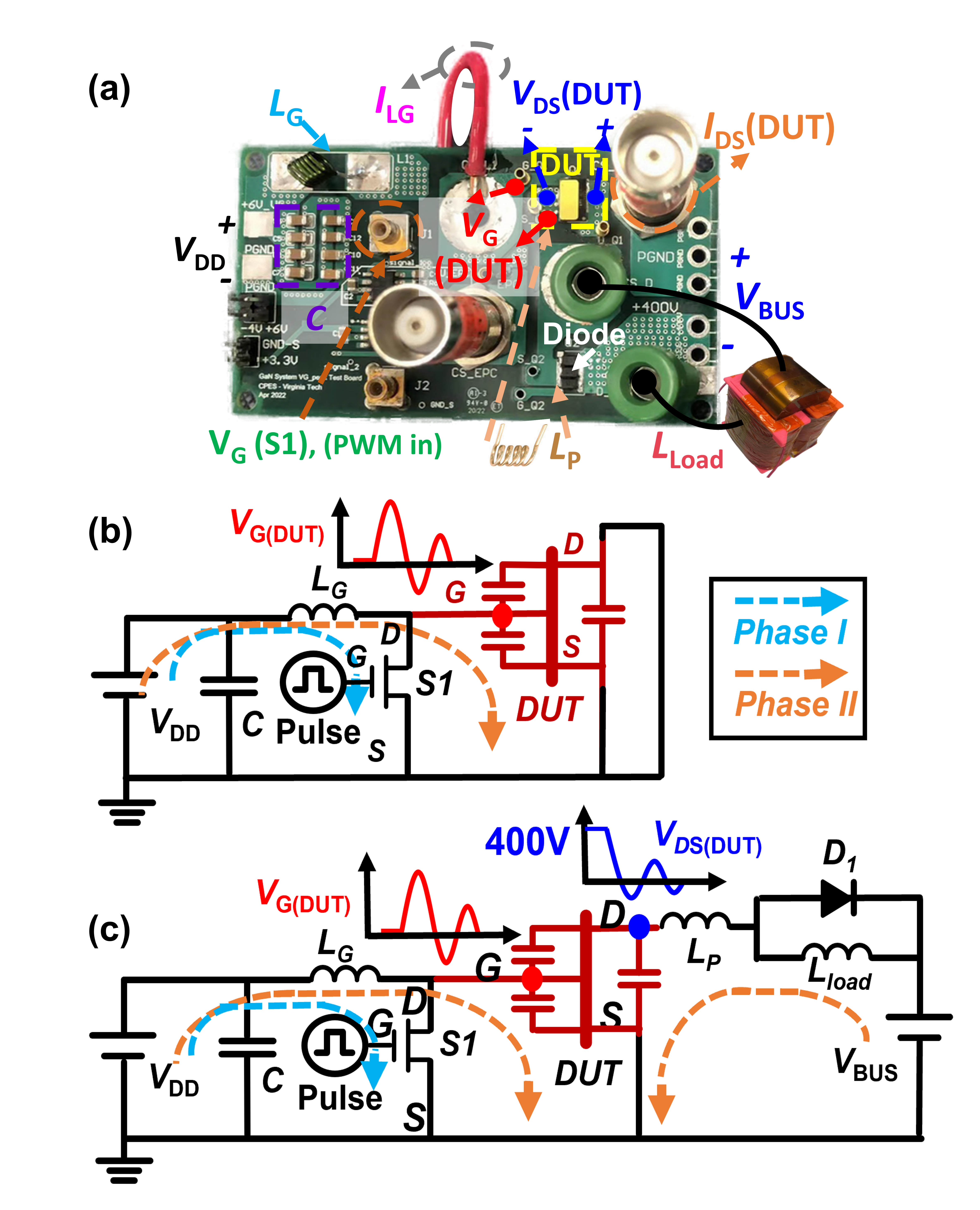
Fig. 1. Proposed circuit: (a) photo, and schematics in (b) drain-and-source grounded condition, and in (c) 400V hard-switching with inductive load condition.
This new circuit method: 1) features a resonance-like VG overshoot with pulse width (PW) down to 20 ns; 2) can achieve the DSG condition for a direct comparison with results from the prior DC and pulse IV methods, as well as the hard switching (HSW) condition at VBUS = 400 V with an inductive load in the drain-source loop to mimic practical conditions.
As shown in Fig. 2, at increased PW, gate BVdyn shows a decrease and then saturation at 21~22 V. Moreover, the gate BVdyn increases with temperature and is higher under hard switching than under the drain-source grounding condition. In the 400 V hard-switching condition at 150 °C, the gate BVdyn reaches 27.5 V.
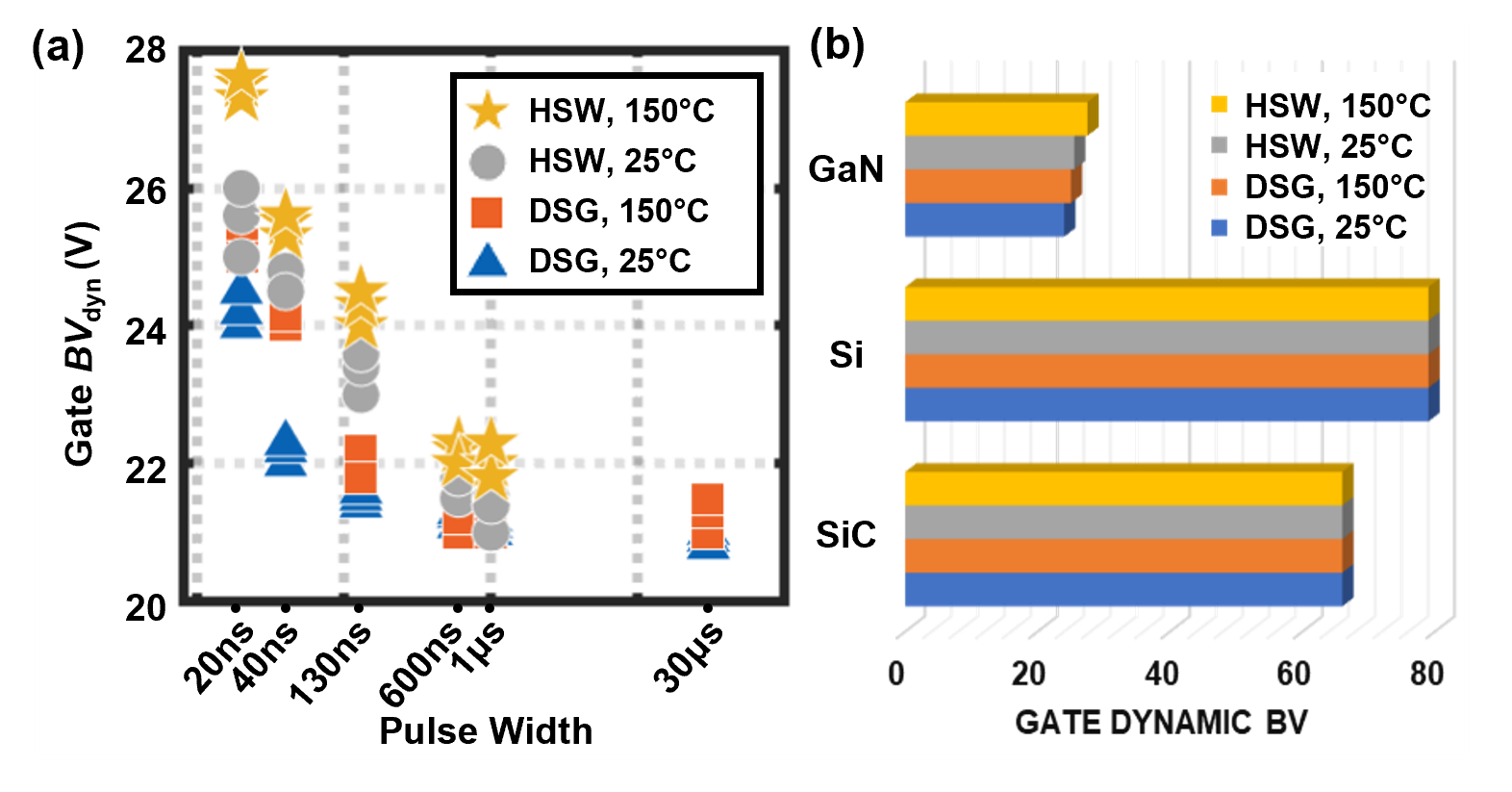
Fig. 2. Test results of gate BVdyn of (a) GaN SP-HEMT, and (b) Si IGBT as well as SiC MOSFET.
Such an impact from the drain-switching locus and temperature on the gate BVdyn is not seen in silicon and silicon-carbide power transistors tested in the same setup (Fig. 2). These results are explained by a decrease in the potential drop across the p-GaN gate stack in hard switching and at high temperatures.
