LIBRARY
Very High Speed Double-Pulse Tester

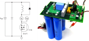
However, more issues need to be concerned when using the double-pulse tester to test high-speed devices. The device switching characteristics should not be affected too much by the test circuit. It has already been shown that the PCB stray inductances will be of great influence to the device switching waveforms if the switching speed is very fast (i.e. switching under very high dv/dt and di/dt). This high-speed double-pulse tester is built by carefully designing the PCB layout to intentionally minimize the most critical parasitic impedances to the device switching, such as the capacitance across the freewheeling diode, the inductances formed by the gate drive loop and the main switching loop, etc.
This double-pulse tester has been used in CPES to test the switching characteristics of both SiC JFET and SiC MOSFET (only with different gate drive circuit for each tester). For SiC JFET, the tester enabled the device to switch with 0 ω gate resistance at a dv/dt rate of 60 kV/us and a di/dt rate of 3 kA/us without causing big ringing, while for SiC MOSFET 20 kV/us and 2 kA/us were achieved. The design considerations for this tester provide a lot of useful insights and guidelines for the ultra-fast gate drive design for SiC switches.


