


LIBRARY
Modeling and Simulation of a High-Temperature SiC JFET/JBS Power Electronics Building Block
Year: 2009
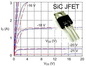
Fig. 1. 1.2 kV, 5 A SiC JFET and its output characteristics.
(Blue solid - measurement; red dashed - simulation).
(Blue solid - measurement; red dashed - simulation).
For active switches, SiC JFETs are the most promising devices to be commercialized in the near future, therefore extensive measurements and tests have been conducted to investigate the performance of the new device, especially the 1.2 kV, 5 A prototypes made by SiCED (Fig. 1). The device characterizations include static characteristics and switching characteristics, from which a SPICE-2 based device model has also been built including all the essential electrical characteristics of the device. From the switching test, the SiC JFET under study is able to switch with zero gate resistance under 600 V, 6 A clamped inductive load, achieving a dv/dt rate of 60 V/ns and a di/dt rate of 3 A/ns, while producing only minor ringing during the ultra-fast switching transients. The model prediction also matches very well with the experimental switching waveforms.
A high-temperature, wire-bond type package for a multi-chip, phase-leg PEBB using all SiC devices have been designed, fabricated and tested to demonstrate the "building block" concept. For the analysis of the module layout design, the package structure has also been modeled using electromagnetic analysis software Ansoft Quick 3D to extract the parasitic impedances, as these parasitics would have great impact on the device during ultra-fast switching transients (Fig. 2). The device and package models can work together in a circuit simulator to display the interactions, which matches the experiments pretty well. This combined simulation can help verify the layout design, showing the influence of the parasitics, and also enable the observation of many hard-to-measure quantities such as current balancing condition and JFET internal current distribution, which are also important design considerations (Fig. 3).
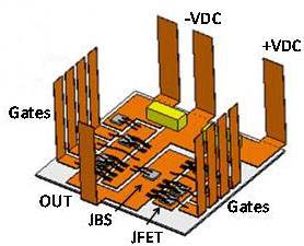
Fig. 2. Q3D model for the SiC JFET/JBS PEBB.
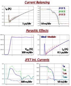
Fig. 3. Device-package combined simulations showing the current balancing, parasitic effects, and JFET internal current distribution.
