Become a Member
Become a Member

LIBRARY

Characterization of Encapsulants for High-Voltage, High-Temperature Power Electronic Packaging

Year: 2010
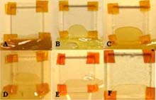
Fig. 1. Flow fronts of potential encapsulants A-F. Glass chip size: 6 mm 6 mm. Pictures were taken within one second of the material being dropped at the edge of the chip.
Seven encapsulants with operating temperature up to 250°C have been surveyed for possible use in high-temperature, high-power planar packages. Processability was assessed by studying the flow fronts and the cured properties of the surveyed materials between paralleled plates. Two encapsulants did not pass the flow test, and another two did not pass the curing test. Material E, F, and G were confirmed to be comparably stable with respect to temperature, and both dielectric strength and dielectric permittivity decreased around 40% and 30%, respectively, as the temperature increased from 25°C to 250°C. The thermal aging test showed that materials were hardened during the aging process, and cracking started in the material matrix. The dielectric strength of the sample would significantly drop to only around 10 kV/mm once cracking occurred.


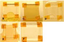
Fig. 2. Textures of materials B-F after the completion of flowing process. Glass chip size: 6 mm 6 mm..
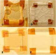
Fig. 3. As-cured textures of materials C-F. Glass chip size: 6 mm 6 mm .
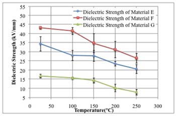
Fig. 4. Temperature dependence of dielectric strength for material E, F, and G.


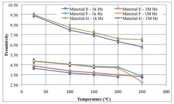
Fig. 5. Temperature dependence of dielectric permittivity of material E, F, and G.
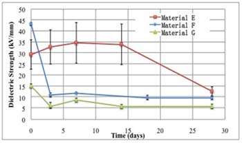
Fig. 6. Dielectric strength of material E, F, and G with respect to aging time.
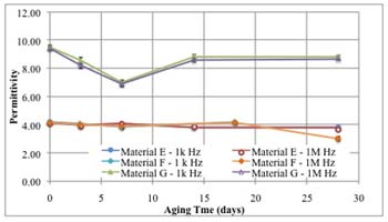
Fig. 7. Permittivity of materials E, F, and G with respect to aging time.

Our Industry Partners