


LIBRARY
The Optimal Design of a GaN-based Dual Active Bridge for a Bi-Directional Plug-in Hybrid Electric Vehicle (PHEV) Charger
Year: 2015
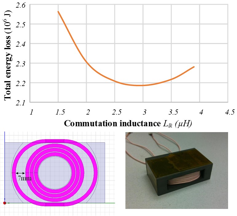
Fig. 1. Commutation inductance selection and the integrated transformer design with integrated commutation inductor
This work first characterizes the GaN multi-chip-module in terms of static and dynamic performances, including forward and reverse conduction characteristics, turn-on and turn-off switching energy, dynamic on-resistance, and output capacitance. A loss model of the DAB converter is thus developed and compared with experimental measurements.
To optimally design the dual active bridge converter, the commutation inductance value must be determined. Since the battery charger has a wide load current and voltage range, the selection criteria of the inductance is to achieve minimum charging loss through the entire charging cycle based on the loss model developed above. The total energy loss through the charging cycle with different commutation inductance is plotted in Fig. 1. Minimum energy loss is obtained when commutation inductance equals 3 µH.
A high frequency transformer with an integrated commutation inductor is built with 3F35 material. A certain amount of space is intentionally left between the interleaved primary and secondary windings so that enough leakage flux can be stored to reach the desired leakage inductance value, as shown in Fig. 1(bottom).
Experimental results of a 500 kHz DAB converter with a discrete inductor and transformer can achieve 97.2% efficiency at 1kW and 96.4% efficiency at 2.4 kW. By integrating the inductor into the transformer, 98.2% efficiency is achieved at 1 kW, as shown in Fig. 2.
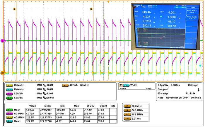
Fig. 2. GaN converter with integrated inductor at 1kW reaches 98.2% efficiency
