LIBRARY
Comparison of Silicon, SiC and GaN Power Transistor Technologies with Breakdown Voltage Rating from 1.2 kV to 15 kV

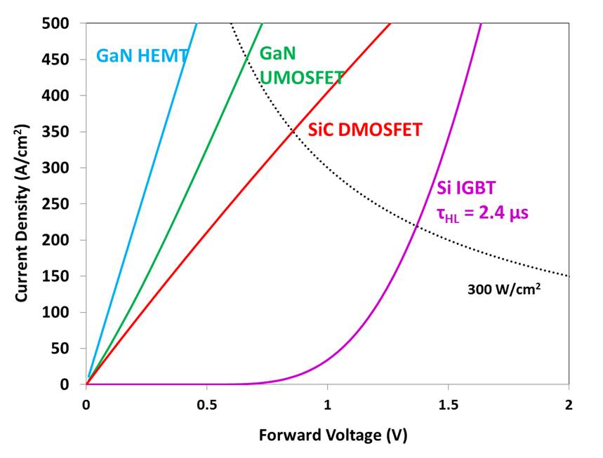
In this study, the devices under consideration are GaN HEMT, SiC MOSFET, GaN MOSFET and Si IGBT at medium voltage ratings (1.2 - 3.3 kV) and GaN MOSFET, SiC MOSFET, SiC IGBT and GaN superjunction HEMT at high voltage ratings (10 - 15 kV). For each device, the drift region has been optimized to support the desired breakdown voltage with minimum on-state resistance. Fig. 1 compares the output I-V characteristics of the transistors rated at 1.2 kV. While GaN HEMTs offers the best performance at 1.2 kV, GaN MOSFETs are the best performers in the 3.3 kV - 10 kV voltage class. This is because at the higher BV rating, the drift layer resistance becomes the dominant component of the total resistance and hence the advantage of having a higher channel mobility (1500 cm2/V.s in the HEMT compared with 100 cm2/V.s in GaN MOS) is diminished. Additionally vertical device architecture is preferred for high voltage applications to minimize the die area. GaN MOSFETs can potentially offer better performance than SiC counterparts due to a higher critical electric field and MOS channel mobil-ity, however the SiC holds the advantage at present in terms of technology maturity and reliabil-ity. At breakdown voltages exceeding 10 kV, the SiC IGBT has lower on-state losses than the unipolar switches because of the conductivity modulation in the drift layer.
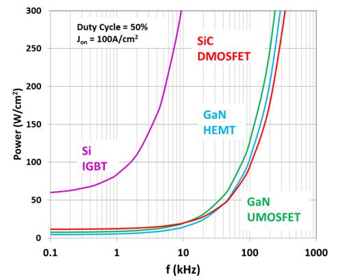
The total power loss (conduction and switching losses, assuming a duty cycle of 50%) is compared for various 1.2 kV transistors as a function of operating frequency. Compared to silicon IGBT, unipolar SiC and GaN transistors have much lower switching losses, which enables these transistors to operate at higher frequencies (by more than one order of magnitude) without increasing power dissipation. Si IGBTs suffer from slow switching speed limited by the re-combination of stored minority carriers. In summary, we have performed a comprehensive simulation study of various wide bandgap power semiconductor switches and silicon IGBTs. In the 600V - 1.2 kV voltage class, GaN HEMTs offer the best performance. As the breakdown voltage increases, vertical device structures become preferable with GaN MOSFETs being the best performer from 3.3 kV to 10 kV. At even higher BV values, SiC IGBTs have the best performance.


