


LIBRARY
System Two-stage Power Architecture for Laptop (2004)
Year: 2004
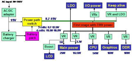
Actually, the laptop has a total load power regulation function to meet the system Thermal Design Power (TDP) requirement. For example, when the laptop detects that the total load power is beyond a certain value, it will lower down CPU clock frequency to reduce CPU power. As a result, although the peak power may exceed the system design power for a very short period, the thermal design power can be greatly reduced. For example, in the above laptop power architecture, the maximum load power can be as high as 110W, but the thermal design power is only about 60W, which is around half of the maximum power. Therefore, if all of the VRs share the same first stage, the first stage thermal design power can be as low as 70W (assuming 85% VR efficiency). To achieve high power density, switching-capacitor voltage divider is used as the 1st stage which has 2000W/in3 power density and 98% efficiency.
Two different designs have been verified by experiments. One design keeps the similar VR cost as the current single-stage solution and improves VR light load efficiency by 5%. Another design has slightly higher VR efficiency comparing with single-stage solution while reducing the footprint of VR output inductors and capacitors by 25%~33% and VR total cost by 5%.
