LIBRARY
Tri-Gate GaN Junction HEMTs: Physics and Performance Space

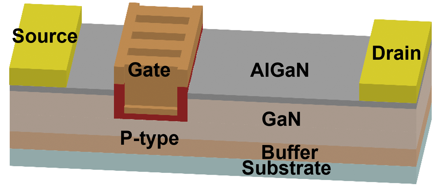
In this work, we comprehensively study the device physics and performance space of GaN Tri-JHEMTs, with the aim to probe their potential advantages over the commercial planar p-gate HEMTs at different voltage classes. 3-D TCAD simulation is employed in this work to traverse a large design space for the p-GaN-based Tri-JHEMT (e.g., fin width, 2DEG density). The simula-tion models are calibrated with the experimental characteristics of the fabricated p-NiO-based Tri-JHEMTs. The experimental characterizations have also demonstrated the first kilovolt blocking capabilities at high temperatures (150 °C) in a GaN trigate HEMTs. These high-temperature char-acteristic show the true variability of Tri-JHEMTs for industrial applications.
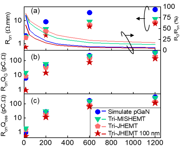
pGaN-based Tri-JHEMT is simulated with calibrated model from NiO Tri-JHEMT experimental results. Comparing with planar pGaN gate HEMT, pGaN Tri-JHEMT allows E-mode with highest wafer 2DEG concentration and lowest sheet resistance. Thanks for the strong gate control capa-bility, Tri-JHEMT can reduce the fin length to ∼100 nm level to reduce gate resistance. Comparing with Tri-MISHEMT, the junction depletion region of Tri-JHEMT removes the parasitic capacitance and minimizes unnecessary gate charges. As shown in Fig. 2, more than 40 % decrease in Ron, RonQG and RonQoss is achieved for Tri-JHEMT at 600 V rating comparing with same gate length planar HEMT. By reducing fin length to 100 nm level, more than 50 % decreasing in above pa-rameters can be obtained for 15 V rating.


