LIBRARY
Gate Driver Switching Noise Propagation Study for Medium Voltage SiC-based Power Electronics Building Blocks

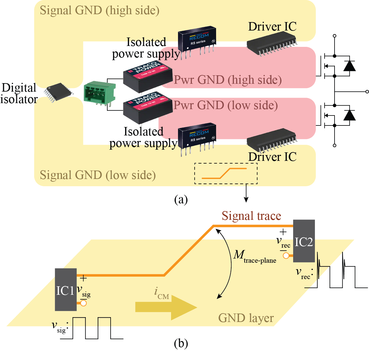
This paper aims to investigate the switching noise propagation on the gate driver PCB under fast dv/dt. Firstly, the dv/dt generated by the power stage induces common-mode (CM) current flowing on the ground layers of the PCB due to the isolation barriers among different PCB grounds (Fig.1(a)). Secondly, the CM noise flowing on ground layers is coupled to the signal traces on other layers which connect between different ICs, due to the mutual inductance be-tween the traces and the ground layer, corrupting the signals that are carried by the traces (Fig.1(b)). The noise at the IC that receives the signal matters. If it exceeds the threshold value of that IC, false triggering will happen.
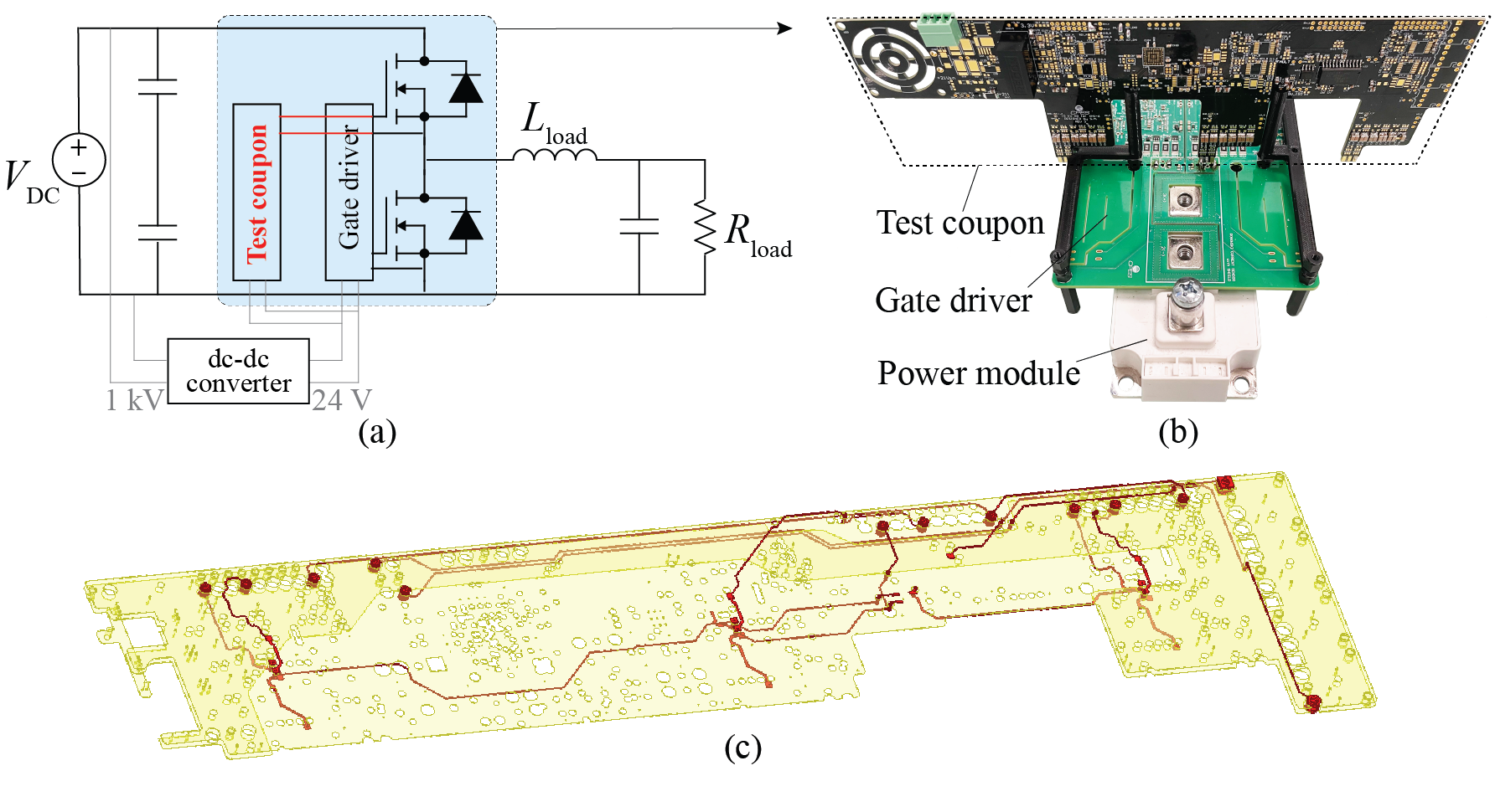
In this paper, an existing gate driver design for a 10 kV power module is used to study how the switching noise is propagated on the gate driver PCB. The study starts with selecting several critical signal traces. FEA simulation is done to find the parasitics of the ground layer and traces, as well as the mutual inductances between them. Experiments are done to comparatively verify the proposed models. It is proved that the noise at the signal receiving IC is strongly related to the trace location, orientation, length and shape.


