LIBRARY
Considerations for Mitigating False Triggering of a Truly Differential Input Gate Driver for 1.2kV SiC MOSFETs

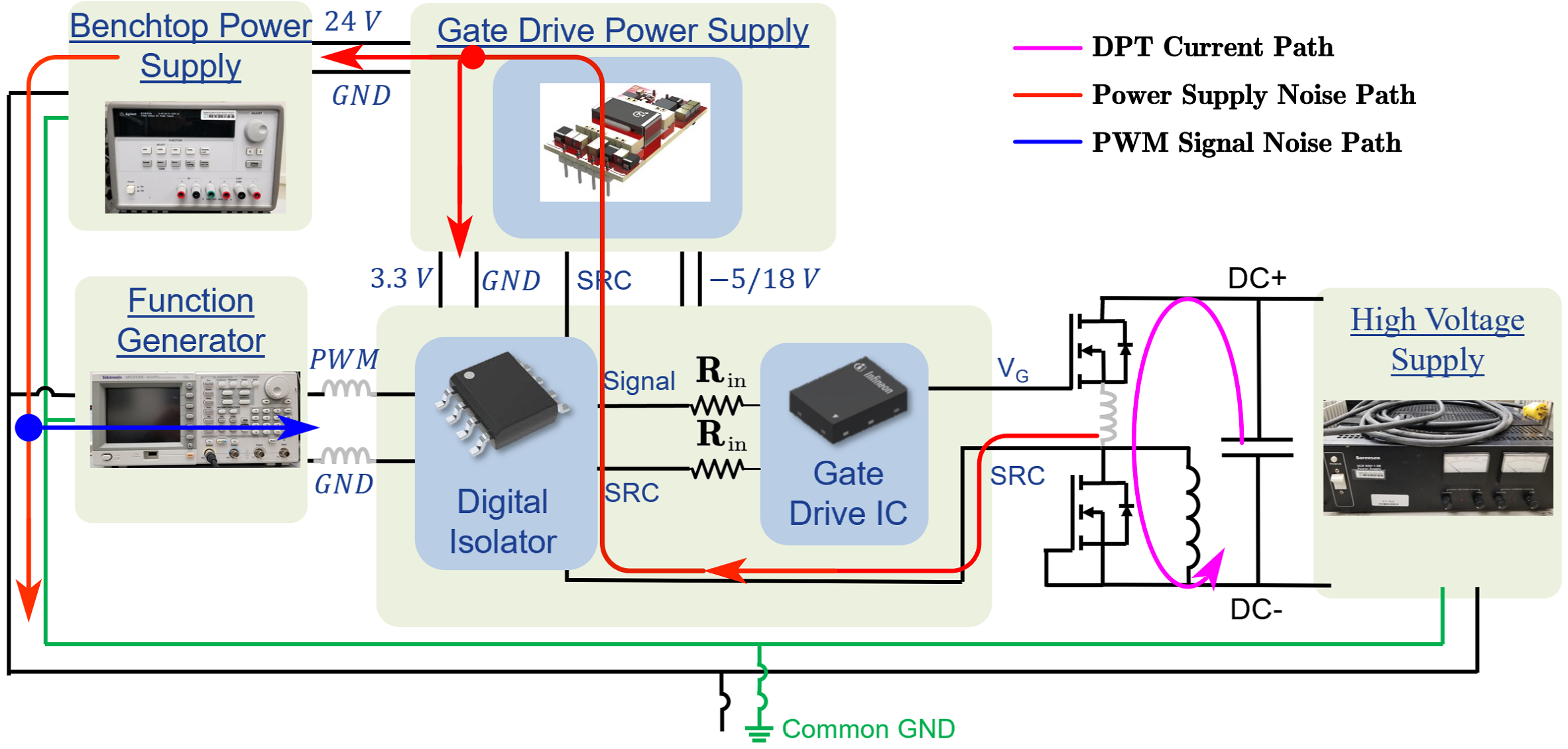
To decouple the PWM signal from the common ground, fiber optic cables were installed, which enabled DPTs to be performed at higher and higher voltages until false triggering was observed at 500 V and 1 A. Modifications to the PCB layout were considered for overcoming the voltage and current limitations. For instance, the differential-pair signal lines were symmetrically routed to help increase CM noise immunity to the input of the gate driver. Furthermore, power planes were converted to traces to eliminate any unintended CM noise paths within the PCB layers. Lastly, a shield plane was added to the last layer of the PCB to provide a path of least resistance and inductance for the transient generated noise to flow away from the sensitive differential-pair signal lines.
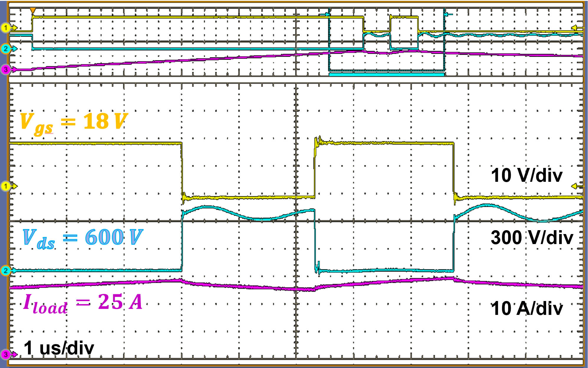
These investigations and solutions enabled DPTs at a drain-to-source voltage of 600 V and a load current of 25 A with no false-turn on events, where a maximum dV/dt of 80 V/ns was achieved. Before the proposed solutions, false triggering was observed at less than 100 V, 5 A at a maximum dV/dt of 16 V/ns.


