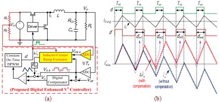
Fig. 1. Proposed digital enhanced V2 control: (a) block diagram; (b) illustrated waveforms.
The basic concept of the V
2 control is utilizing the equivalent series resistor (ESR) of the output capacitors as a virtual current sensing resistor to inherently achieving current mode control with the only output voltage feedback. However, for the converters with small ESR capacitors, such as ceramic capacitors, the conventional V
2 control suffers from the pulse-skipping ripple oscillation instability due to the lagging phase of the output voltage ripple relative to the inductor current ripple. In order to eliminate the ripple oscillation instability, an external ramp compensation strategy has been proposed. However, the system with an external ramp can't be well-damped. Another method is to directly sense the inductor current by using a sensing resistor or DCR current sensing techniques to reduce the relative phase lag of the output voltage ripple due to low ESR capacitors. However, sampling inductor currents normally involves high-resolution and high sampling-rate analog-to-digital converters (ADCs) for avoiding the limit-cycle oscillation Instead of directly sensing the inductor current, derivative-output voltage based methods have also been presented. However, the sensing signal from the derivative output voltage suffers from the distortion issue due to the existing ESR of the output capacitors. Though the derivative-output based methods provide an alternative solution for the instability with analog circuitry implementation, it is still challenging and attractive to find a practical solution with digital implementations since the differentiation process needs high sampling-rate ADCs and may suffer from high-frequency noise problems.
This innovation proposes a new digital enhanced V
2 control architecture with an inductor current ramp estimator for buck converters with low-ESR capacitors without directly sensing the inductor current as shown in Fig. 1. Only the input and output voltages are required to be fed back to the controller, and the inductor current ramp can be estimated as using a high sampling rate (up to the system clock) ADC for sampling the inductor current for stabilizing the system. Actually, only a low sampling-rate ADC is required to sample the input voltage, and the resolution requirement for the ADC is not critical. In this innovation, a compensation strategy for avoiding the drift issue is presented to track the preset valley current level at the steady states. With compared to the external ramp, the estimated current ramp works as an internal ramp, since it contain the current transient information during the load transients by synchronizing to the DPWM. Fig. 1(b) illustrates the operational waveforms of the current ramp estimation with the drift compensation during the steady-state operations.


